General Introduction
This section contains a quick overlook on the general properties of the JUNGFRAU detector, in order to better understand its properties, the way to control it and its output, independently from the specific installation.
JUNGFRAU basics
The ASIC
JUNGFRAU is a hybrid pixel detector designed and produced at Paul Scherrer Insitut (PSI) [1], in Villigen (CH), consisting of pixelated ASICs bump-bonded to a semiconductor sensor (tipically 320 \(\mu m\) thick Si, but 450 \(\mu m\) is also available, and the use of high-Z materials like CdZnTe and GaAs is currently under study).
Its pixel pitch is of 75 \(\mu m\) and it features a charge integrating Dynamic Gain Switching (DGS) architecture, which grants it a dynamic range of the order 110 dB. Each pixel has an array of 16 memory cells that can store the analog signal before the readout.
The pixels are assembled in ASICs of \(256 \times 256\) pixels, which are in turn assembled in an array of \(4 \times 2\) chips, constituting a single JUNGFRAU module of 1024 columns and 512 rows, for a total of about 500 thousand pixels.
Each ASIC is divided in supercolumns of 64 columns \(\times\) 256 rows, whose pixel output signal is multiplexed to an individual off-chip Analog to Digital Converter (ADC) for digitization; the whole module is therefore read out by a total of 32 different ADCs.
The readout board
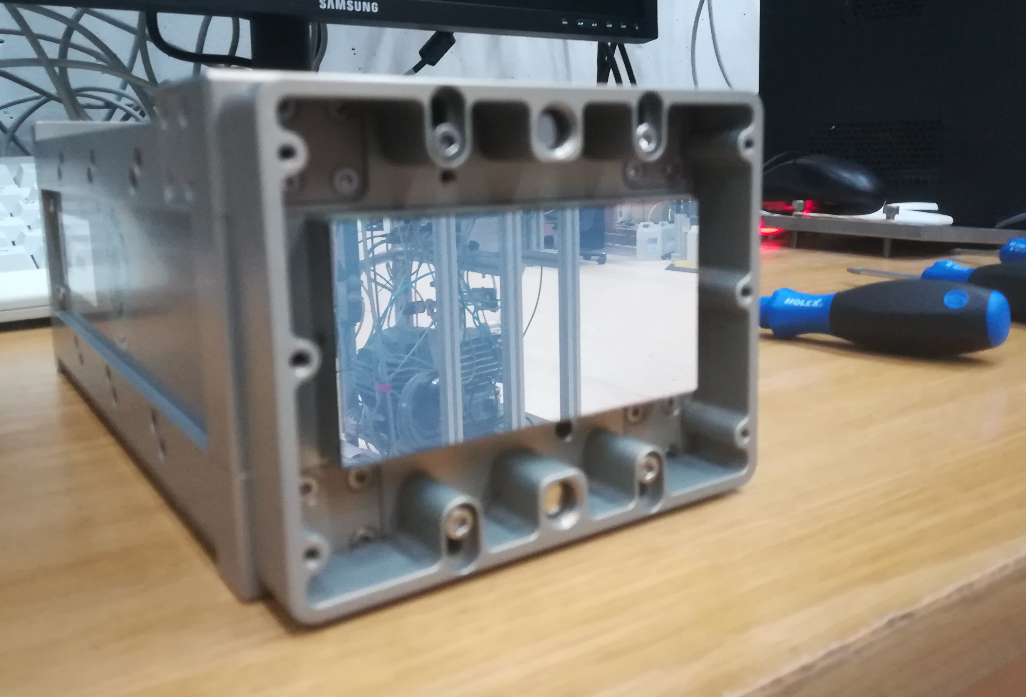
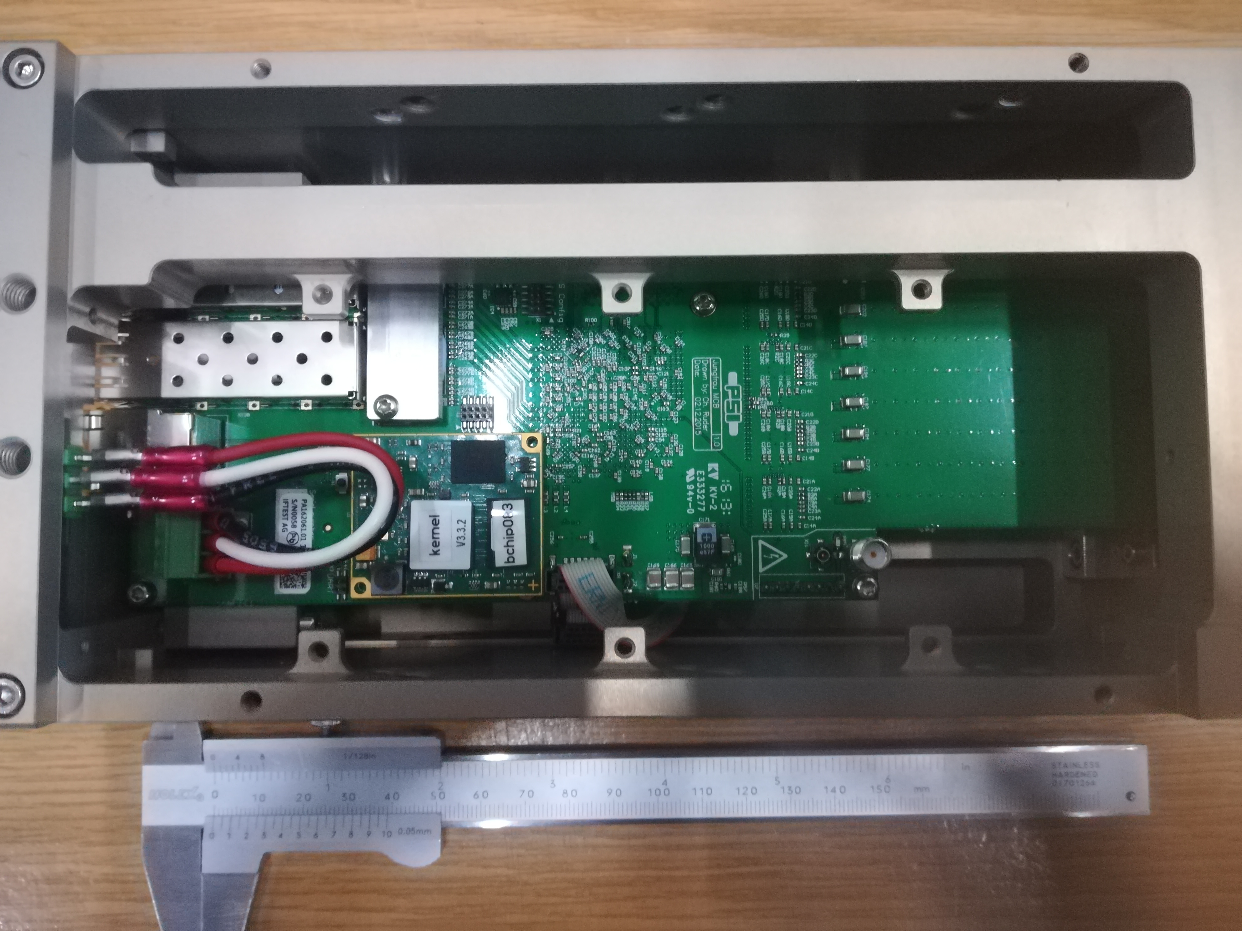
The module read out and control is performed via the JUNGFRAU board (see Fig. 2), an electronic component also provided by PSI, which connects directly to the front end module. The slow control is performed through a server (jungfrauDetectorServer) running on a PC mounted on the board running a LINUX-based OS, and a receiver running on a local physical host. The jungfrauDetectorServer allows to control an FPGA (also mounted on the JUNGFRAU board), which in turn regulates the operation of the ASICs, by starting and stopping the acquisition, and changing certain parameters in between runs, e.g.:
- integration time;
- number of trains;
- operation mode (DGS or fixed gain);
- self-trigger or external trigger.
External and internal triggering
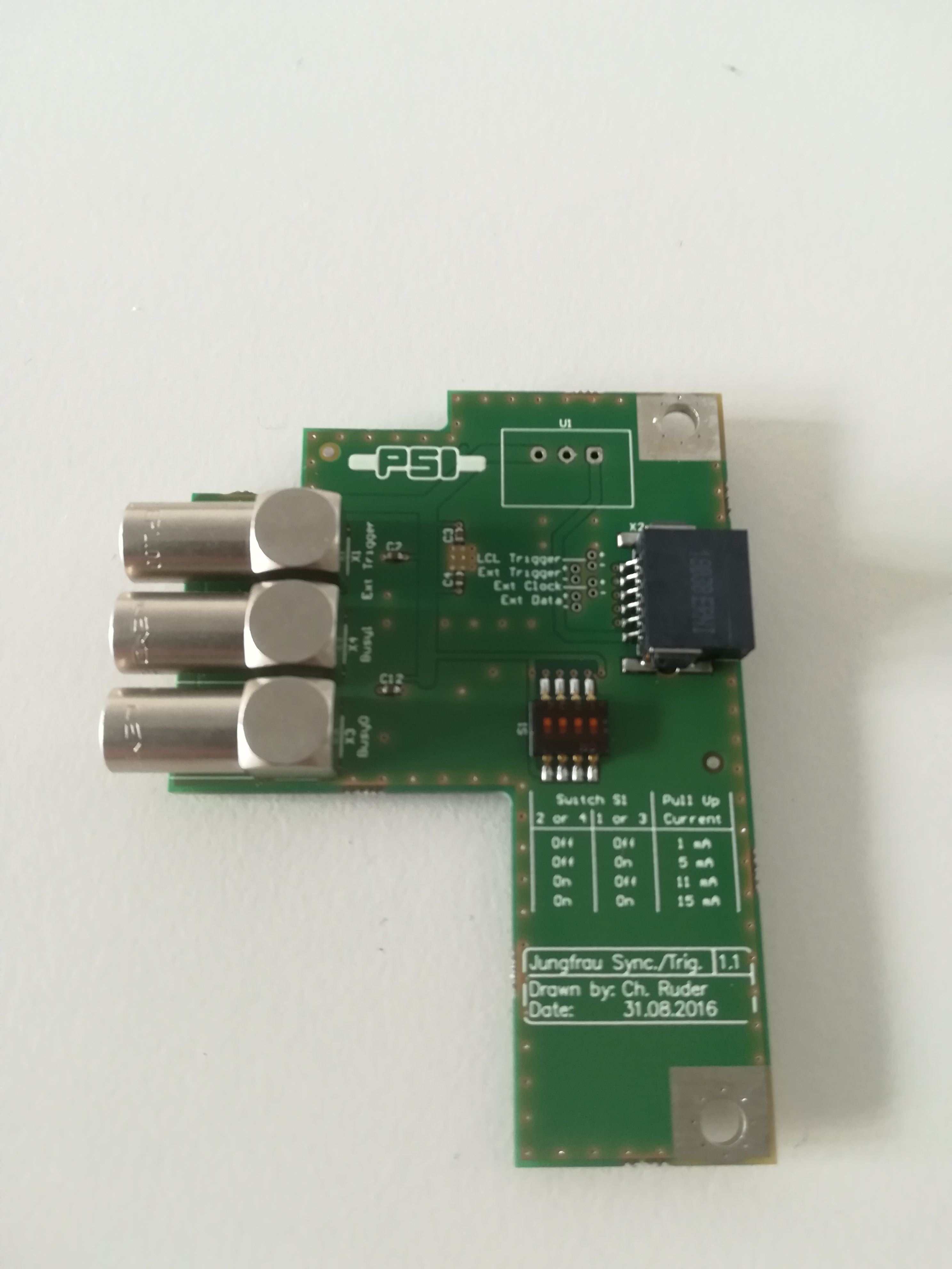
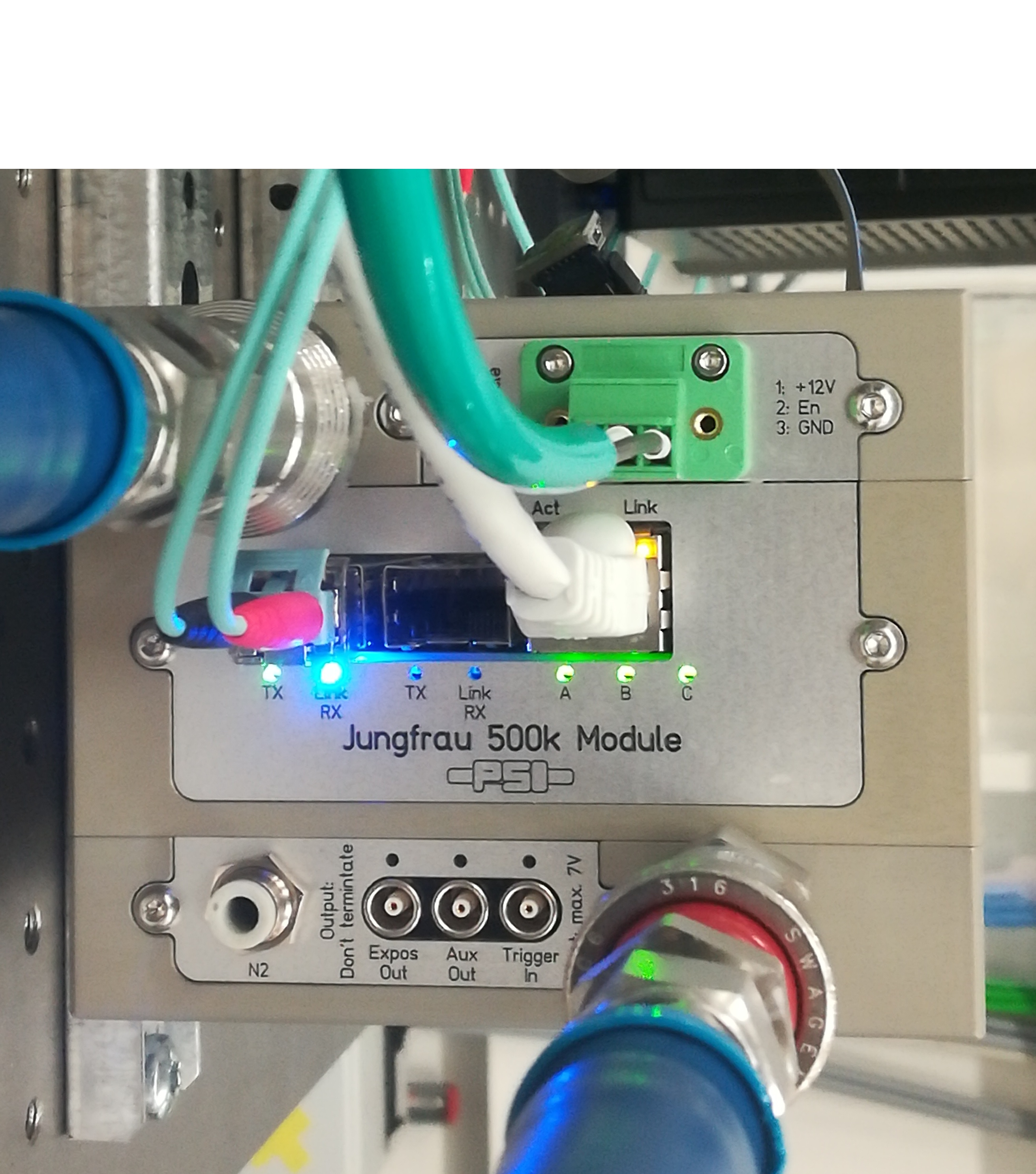
A module can run in autotrigger mode, with read out period adjustable by the user, or, as it will almost always be the case at the European XFEL, in external trigger mode. In this second case, each module must be triggered independently, with a TTL signal whose top-up part is at least 100 ns long. The external signal is converted and delivered to the JUNGFRAU board through an additional triggering board (see Fig. 3), with three LEMO ports: trigger in, trigger out, and one port without a reserved signal yet (see Fig. 4).
Cooling
The module temperature must be kept stable by external cooling: each FEM module dissipates about 20 W, and the amount increases to about 36 W including the readout electronics. It is therefore strongly not recommended the module operation without a functioning cooling system in place: the performances of the detector will certainly suffer (pedestal stability, noise, etc.), and damage to the components may occur. For normal operation, a temperature of the cooling fluid between 15 \(^{\circ}C\) and 20 \(^{\circ}C\) is suggested. It is also recommended not to vary the set temperature during operation.
Dynamic Gain Switching and Raw output
This section focuses on outlining the generalities of the DGS mechanism as implemented in the JUNGFRAU detector, to better understand the treatment of raw data needed in order to convert the ADC output in physical units.
Dynamic Gain Switching
In order to comply with the dynamic range requirements of a FEL, the pixel architecture of the JUNGFRAU detector is designed with a dynamic gain switching mechanism similar to the one implemented in the AGIPD detector: a pixel-wise threshold comparator switches in additional feedback capacitors in the pre-amplifier if the signal is above a certain value (set module-wise by the factory), thus increasing the feedback capacitance and reducing the gain. There are a total of three subsequent gain stages which can be independently triggered in each pixel, depending on the incoming signal:
- G0, which goes from single photon sensitivity up to a signal of about 20 - 25 10 keV photons;
- G1, which goes up to 500 - 600 10 keV photons;
- G2, which goes up to 8000 - 10000 10 keV photons.
Additionally, there is a fourth gain stage available:
- HG0 (High Gain Zero), which can be statically set for the whole module as first gain stage in place of G0; it has an amplification factor roughly five times higher than G0; this can grant better single photon resolution, at the price of a reduced resolution for multiple events, because the pixel will switch to G1 only after a signal equivalent to 4 - 5 10 keV photons.
The state of the DGS mechanism is recorded memory cell-wise and for every raw image a corresponding gain bit map is produced, which indicates whether each pixel was in G0, G1 or G2 at the end of the integration time.
Raw data output
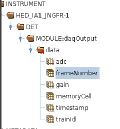
Fig. 5 The data structures that will be found in each hdf5 file, at the path corresponding to the RECEIVER device
Therefore, the data structures that will be found in each hdf5 file that contains the output of a JUNGFRAU module are shown in Fig. 5 and consist of:
- adc contains the raw ADC output and is an array of 16-bit integers, with the following shape: (trains, memorycells, rows, columns);
- gain contains the gain bit value (16-bit integer) registered by the threshold comparator at the end of the exposure time; it has the same dimensions of adc;
- timestamp is an array of 64-bit floats, as long as many trains in the file, indicating the time stamping of each one of them;
- trainId an array of 64-bit integers, with the train ID associated to each acquired train contained in the file;
- frameNumber is the output of the internal frame counter of each module; this count will reset after reboot;
- memoryCell an array 16-bit integers, ranging from 0 to 15, indicating the cell ID of the corresponding image.
Due to some technicality in the chip design, the polarity of the signal after the first gain switching is inverted; this means that:
- for G0, increasing input signal corresponds to increasing ADC output, and the values will range from ~ 2000 ADC units (average offset with 10 \(\mu s\) integration time) up to ~ 13000 ADC units (the average gain switching point);
- for G1 and G2, the opposite is true: for increasing input signal, the ADC output decreases, which means that the raw output values will range from a minimum of ~14000 ADC units (average offset value) down to 0 - 1000 ADC units for high signals.
An example can be seen in Fig. 6.
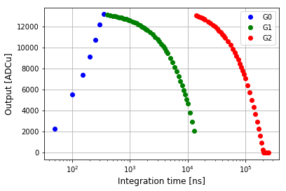
Fig. 6 Example of pixel switching gains during an internal current source scan, when the pixel gain switching mechanism is calibrated by providing a constant current and increasing the integration time
As a consequence, the offset subtracted output without gain calibration correction will return positive values for the pixels in G0, and negative values for the ones in G1 or G2. This feature of the detector must be taken in consideration while inspecting the corrected output data: if no gain correction has been applied, and substantial parts of the images are in the middle or low gain stage, the physical interpretation of the output may be difficult to subsume.
In order to convert the raw JUNGFRAU ADC output into physical unit, the following constants are needed:
- a memory cell-wise map of the gain calibration correction factors, for each gain stage; these maps exist for each module and provide these factors in ADC units/keV;
- a memory cell-wise map of the offset to subtract from the raw output, for each gain stage; the offset varies with the integration time, therefore such maps must be calculated from dark runs expressly taken every time the integration time has changed.
With both these pieces of information available, the procedure to convert the raw data into physical units is therefore:
- for each image, the corresponding gain bit map is used to understand at which gain stage each pixel is;
- on a memory cell by memory cell basis, the offset corresponding to the proper gain stage must be subtracted from the raw output;
- on a memory cell by memory cell basis, the offset-subtracted ADC value must be converted into physical units, dividing it by the corresponding gain conversion factor.
The gain calibration constants are, for each module present at the EuXFEL, inserted in the calibration database, and so are the corresponding offsets. New offset values can however be easily calculated from dark runs and subsequently injected in the database; details of the procedure are explained in Data Correction.
| [1] | https://www.psi.ch/de/lxn/jungfrau |
