3. Dark Characterization
This chapter presents an overview of the characterization of the dark data obtained with the new pnCCD detector.
3.1. Nomenclature
Following the original nomenclature used for CCD analysis performed by Steffen Hauf at European XFEL for FastCCD and pnCCD notebooks, the pnCCD detector is defined to be a matrix of 1024 rows by 1024 columns. Here, every row is horizontal and every column is vertical. In other words, rows and columns are defined by axis \(= 0\) and axis \(= 1\) in standard PYTHON definition, respectively. Since the pnCCD readout is horizontal, charge is collected per row. Also, each pixel along a column is readout in parallel and at the same time.
Note
- The above nomenclature is not the same as that used by the PNSensor. They follow the standard CCD nomenclature and define the detector as a matrix of 1024 columns by 1024 lines, where their columns correspond to our rows and each line is the same as what we define to be a column. This manual uses our nomenclature instead of that used by the PNSensor.
3.2. Empty Frames
With the pnCCD notebooks developed at European XFEL, we normally read the data in chunks of 100 frames. It then follows that regardless of the pnCCD gain, if the duration of a dark run is less than 500 trains or frames, there will be empty frames at the end of the run. In this case, the number of empty frames will be:
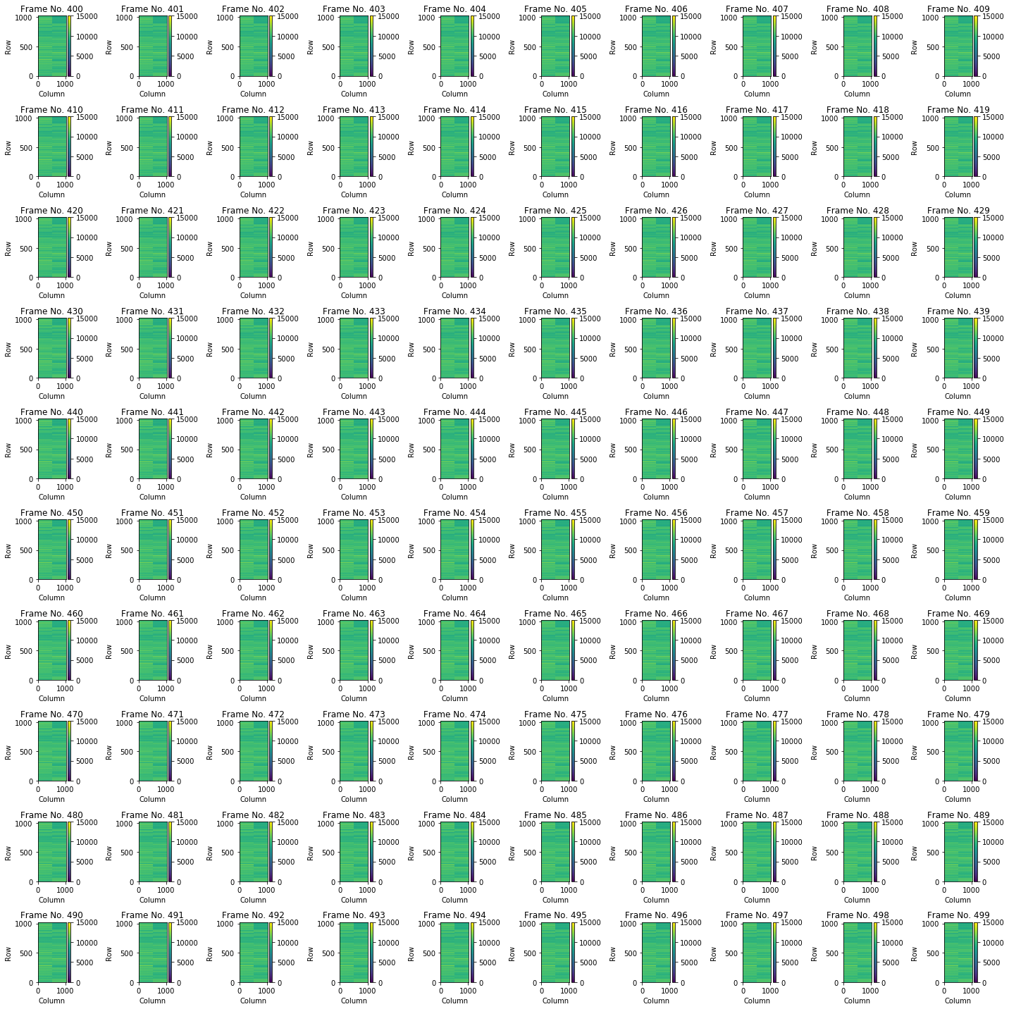
where \(EF\) is the number of empty frames appearing towards the end of the run, and \(n\) is the actual number of acquired trains or frames. Fig. 3.1 shows an example of a case where the number of acquired dark frames are fewer than 500, and thus there are empty frames at the end of the run. Fig. 3.2 shows an example of having 500 trains for a dark run, and thus there are no empty frames.
Warning
- It is important to search for and exclude the empty frames prior to calculation of the offset; otherwise, the mean signal (averaged over number of frames) per pixel will be affected by the empty frames whose signal values are zero for all pixels.
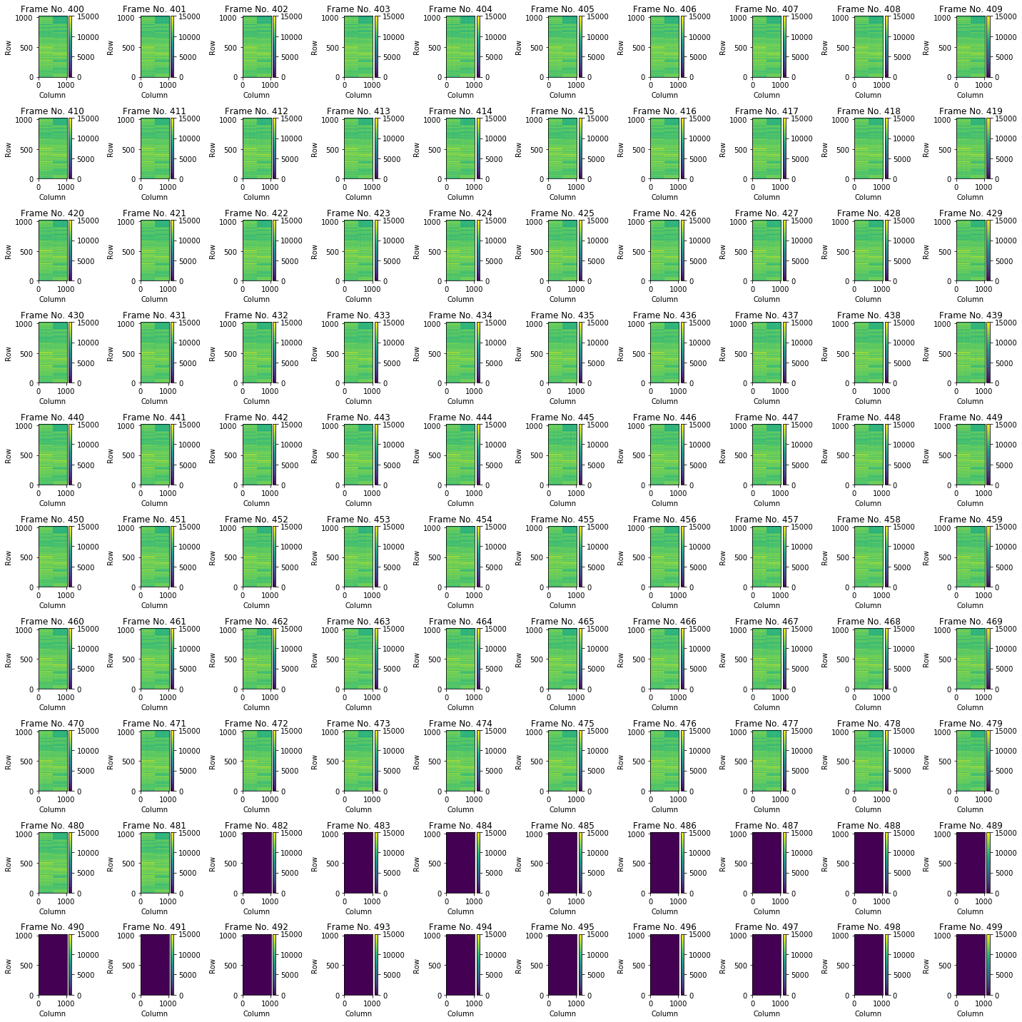
Fig. 3.1 An overview plot showing the last 100 raw (no corrections applied) dark image frames of run number 1 from proposal 2714. In this case the last 18 image frames are empty because the total number of frames in this run were 482 instead of 500. These 18 empty frames need to be excluded prior to calculating the offset.
3.3. pnCCD Offset
Offset is the same as the dark pedestal. Regardless of the pnCCD mode of operation, the dark offset per pixel is calculated as:
where \(N\) is the total number of frames acquired in the dark run, and \(Pixel\,Signal\) is the value (in ADU) for each pixel of the pnCCD detector. Therefore, the dark offset per pixel is the pixel signal averaged over the number of frames acquired in a dark run. Since pnCCD has 1024 \(\times\) 1024 pixels, a matrix of the offset per pixel for all these pixels is known as the offset map (see Fig. 3.3). To calculate the offset map, we normally only consider up to 500 frames (sequence 0) even if there are more frames stored in the raw data files, i.e., there are more than one sequences. The offset map is calculated after rejecting the empty frames. Generally, the offset map shows a horizontal stripe structure along the CCD readout axes (see Fig. 3.3). This is expected for a pnCCD-type detector with a horizontal parallel readout.
At the moment, the bad pixels (see BadPixels), including the area of the central hole, is not excluded prior to the calculation of the dark offset map. However, excluding bad pixels surprisingly changes the offset map only by a small amount (see Fig. 3.34). Of course, if there are too many bad pixels, the change in the offset map and its average value over all pixels may be a bit more noticeable. For example, the dark run number 361 from proposal 900166 has an average offset (over the entire detector) of 11522.78 \(\pm\) 809.22 ADU if we do not exclude the bad pixels. But this value is reduced to 11505.59 \(\pm\) 767.40 ADU after exclusion of all bad pixels. In this case, the detector was exposed to a high intensity of scattered X-rays for a relatively long time before taking the dark run. This caused a dramatic increase in the number of hot (noisy) pixels near the central hole. Consequently, excluding these bad pixels has a more noticeable effect on the acquired dark offset.
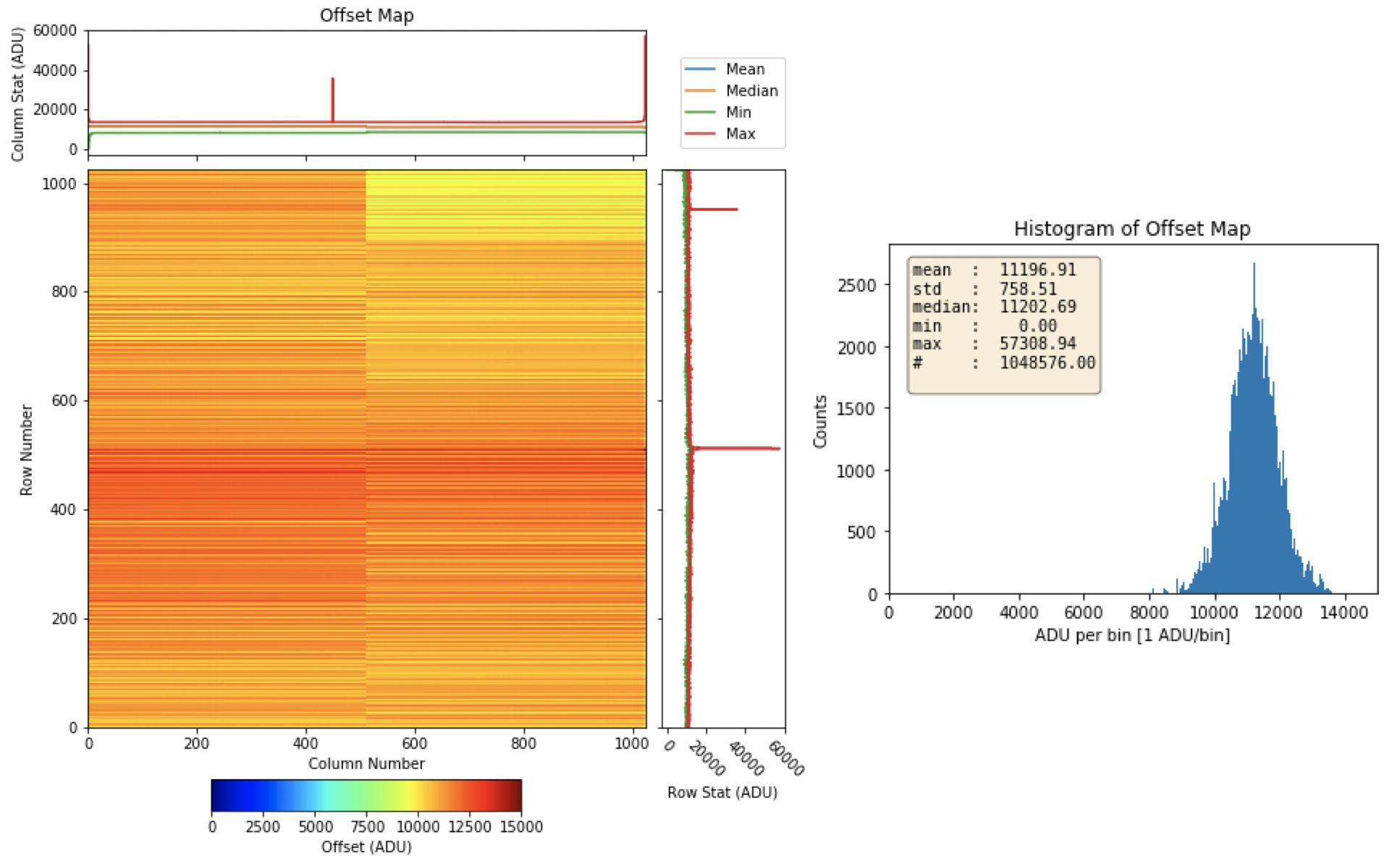
Fig. 3.3 (Right) Offset map, and (left) histogram of the offset map for save mode of operation with bias voltage of \(- 270\) V and gain configuration of 1/1. Data are from run 1 in proposal 2714.
3.3.1. Save Operation Mode
The pnCCD detector has 3 modes of operation:
- Save mode
- Normal mode
- High Dynamic Range (HDR) mode
Each of these modes has a different bias voltage and is to be used for a different purpose (see pnCCD Operation Manual). In this section, we present the dark offset characteristics of the Save Mode of operation.
Table 3.1 summarizes the mean offset for the individual CCD quadrants and for the whole detector for different gain configurations in the save mode. Fig. 3.3 shows an example of the offset map and its histogram for this mode of operation. The histogram binning is performed such that each bin has 1 ADU.
| Gain | Detector Region | Offset | Operation Mode |
| 1/1 | Whole Detector | 11196.91 \(\pm\) 758.51 ADU | Save |
| Lower Left Quadrant | 11111.63 \(\pm\) 578.64 ADU | ||
| Upper Left Quadrant | 11597.80 \(\pm\) 685.09 ADU | ||
| Lower Right Quadrant | 10701.73 \(\pm\) 735.06 ADU | ||
| Upper Right Quadrant | 11376.50 \(\pm\) 715.13 ADU | ||
| 1/4 | Whole Detector | 10415.13 \(\pm\) 619.75 ADU | Save |
| Lower Left Quadrant | 10446.11 \(\pm\) 529.52 ADU | ||
| Upper Left Quadrant | 10693.92 \(\pm\) 543.75 ADU | ||
| Lower Right Quadrant | 10086.76 \(\pm\) 621.49 ADU | ||
| Upper Right Quadrant | 10433.72 \(\pm\) 622.23 ADU | ||
| 1/16 | Whole Detector | 10185.49 \(\pm\) 595.67 ADU | Save |
| Lower Left Quadrant | 10251.94 \(\pm\) 527.13 ADU | ||
| Upper Left Quadrant | 10425.33 \(\pm\) 520.04 ADU | ||
| Lower Right Quadrant | 9894.64 \(\pm\) 598.83 ADU | ||
| Upper Right Quadrant | 10170.06 \(\pm\) 604.67 ADU | ||
| 1/64 | Whole Detector | 10121.99 \(\pm\) 589.66 ADU | Save |
| Lower Left Quadrant | 10196.98 \(\pm\) 526.19 ADU | ||
| Upper Left Quadrant | 10352.53 \(\pm\) 514.16 ADU | ||
| Lower Right Quadrant | 9841.56 \(\pm\) 592.65 ADU | ||
| Upper Right Quadrant | 10096.90 \(\pm\) 600.25 ADU | ||
| 1/256 | Whole Detector | 10109.32 \(\pm\) 588.43 ADU | Save |
| Lower Left Quadrant | 10186.05 \(\pm\) 526.35 ADU | ||
| Upper Left Quadrant | 10338.04 \(\pm\) 513.12 ADU | ||
| Lower Right Quadrant | 9832.37 \(\pm\) 591.23 ADU | ||
| Upper Right Quadrant | 10080.83 \(\pm\) 599.49 ADU | ||
| 1/340 | Whole Detector | 10113.11 \(\pm\) 588.36 ADU | Save |
| Lower Left Quadrant | 10186.05 \(\pm\) 526.35 ADU | ||
| Upper Left Quadrant | 10338.04 \(\pm\) 513.12 ADU | ||
| Lower Right Quadrant | 9832.37 \(\pm\) 591.23 ADU | ||
| Upper Right Quadrant | 10080.83 \(\pm\) 599.49 ADU | ||
| 1/512 | Whole Detector | 10117.59 \(\pm\) 588.36 ADU | Save |
| Lower Left Quadrant | 10191.80 \(\pm\) 526.57 ADU | ||
| Upper Left Quadrant | 10350.57 \(\pm\) 510.58 ADU | ||
| Lower Right Quadrant | 9842.72 \(\pm\) 590.51 ADU | ||
| Upper Right Quadrant | 10085.29 \(\pm\) 601.35 ADU |
3.3.2. Normal Operation Mode
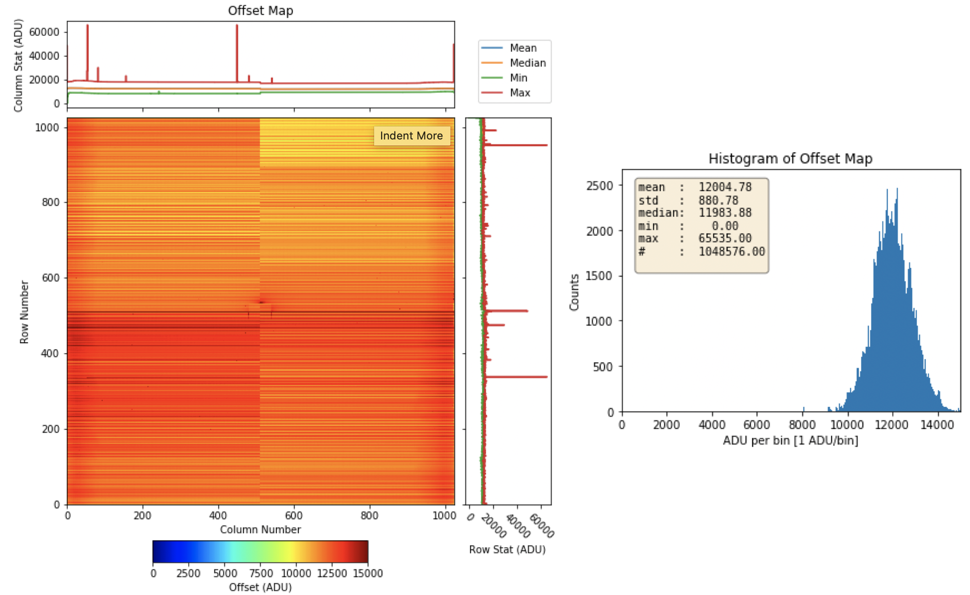
In this section, we present the dark offsets corresponding to the normal mode of operation. Table 3.2 summarizes the mean offset for the individual CCD quadrants and for the whole detector for different gain configurations in the normal mode of operation. Fig. 3.4 shows an example of the offset map and its histogram for the normal mode of operation. The histogram binning is performed such that each bin has 1 ADU.
| Gain | Detector Region | Offset | Operation Mode |
| 1/1 | Whole Detector | 12004.78 \(\pm\) 880.78 ADU | Normal |
| Lower Left Quadrant | 11671.47 \(\pm\) 639.61 ADU | ||
| Upper Left Quadrant | 12674.40 \(\pm\) 722.17 ADU | ||
| Lower Right Quadrant | 11350.65 \(\pm\) 745.44 ADU | ||
| Upper Right Quadrant | 12322.61 \(\pm\) 726.88 ADU | ||
| 1/4 | Whole Detector | 10630.91 \(\pm\) 635.43 ADU | Normal |
| Lower Left Quadrant | 10599.78 \(\pm\) 540.68 ADU | ||
| Upper Left Quadrant | 10970.12 \(\pm\) 574.14 ADU | ||
| Lower Right Quadrant | 10263.55 \(\pm\) 622.48 ADU | ||
| Upper Right Quadrant | 10690.19 \(\pm\) 617.60 ADU | ||
| 1/16 | Whole Detector | 10256.59 \(\pm\) 597.49 ADU | Normal |
| Lower Left Quadrant | 10306.39 \(\pm\) 528.65 ADU | ||
| Upper Left Quadrant | 10506.06 \(\pm\) 522.44 ADU | ||
| Lower Right Quadrant | 9957.12 \(\pm\) 598.52 ADU | ||
| Upper Right Quadrant | 10256.78 \(\pm\) 602.44 ADU | ||
| 1/64 | Whole Detector | 10153.17 \(\pm\) 589.63 ADU | Normal |
| Lower Left Quadrant | 10223.67 \(\pm\) 526.57 ADU | ||
| Upper Left Quadrant | 10380.26 \(\pm\) 517.21 ADU | ||
| Lower Right Quadrant | 9871.63 \(\pm\) 592.69 ADU | ||
| Upper Right Quadrant | 10137.12 \(\pm\) 598.79 ADU | ||
| 1/256 | Whole Detector | 10129.58 \(\pm\) 587.97 ADU | Normal |
| Lower Left Quadrant | 10204.55 \(\pm\) 526.44 ADU | ||
| Upper Left Quadrant | 10351.47 \(\pm\) 516.16 ADU | ||
| Lower Right Quadrant | 9874.09 \(\pm\) 591.32 ADU | ||
| Upper Right Quadrant | 10109.20 \(\pm\) 598.26 ADU | ||
| 1/340 | Whole Detector | 10131.78 \(\pm\) 587.70 ADU | Normal |
| Lower Left Quadrant | 10206.06 \(\pm\) 526.14 ADU | ||
| Upper Left Quadrant | 10355.08 \(\pm\) 514.56 ADU | ||
| Lower Right Quadrant | 9856.73 \(\pm\) 591.48 ADU | ||
| Upper Right Quadrant | 10109.27 \(\pm\) 598.82 ADU | ||
| 1/512 | Whole Detector | 10134.66 \(\pm\) 587.41 ADU | Normal |
| Lower Left Quadrant | 10208.14 \(\pm\) 526.18 ADU | ||
| Upper Left Quadrant | 10359.87 \(\pm\) 512.95 ADU | ||
| Lower Right Quadrant | 9861.04 \(\pm\) 590.79 ADU | ||
| Upper Right Quadrant | 10109.61 \(\pm\) 599.65 ADU |
3.3.3. High Dynamic Range Operation Mode
In this section, we present the dark offsets corresponding to the HDR mode of operation. Table 3.3 summarizes the mean offset for the individual CCD quadrants and for the whole detector for different gain configurations in the HDR mode of operation. Note that the data corresponding to gain 1/4 presented in Table 3.3 are obtained from a dark run taken during a different day than those of other gains. This is why, the dark offset of this particular run is slightly different from those of other runs presented in Table 3.3. The dark run corresponding to gain 1/4 was taken after the pnCCD was exposed to high intensity for a while, and thus around the central hole region, there was a lot of hot pixles, which ended up increasing the dark offset value.
Fig. 3.5 shows an example of the offset map and its histogram for HDR mode of operation. The histogram binning is performed such that each bin has 1 ADU.
| Gain | Detector Region | Offset | Operation Mode |
| 1/1 | Whole Detector | 11522.12 \(\pm\) 811.40 ADU | High Dynamic Range |
| Lower Left Quadrant | 11395.99 \(\pm\) 614.13 ADU | ||
| Upper Left Quadrant | 11943.23 \(\pm\) 746.20 ADU | ||
| Lower Right Quadrant | 11028.56 \(\pm\) 823.88 ADU | ||
| Upper Right Quadrant | 11720.68 \(\pm\) 737.88 ADU | ||
| 1/4 | Whole Detector | 10585.31 \(\pm\) 661.45 ADU | High Dynamic Range |
| Lower Left Quadrant | 10695.45 \(\pm\) 644.18 ADU | ||
| Upper Left Quadrant | 10792.36 \(\pm\) 562.41 ADU | ||
| Lower Right Quadrant | 10314.27 \(\pm\) 704.65 ADU | ||
| Upper Right Quadrant | 10539.16 \(\pm\) 625.86 ADU | ||
| 1/16 | Whole Detector | 10221.26 \(\pm\) 596.75 ADU | High Dynamic range |
| Lower Left Quadrant | 10282.53 \(\pm\) 528.70 ADU | ||
| Upper Left Quadrant | 10456.20 \(\pm\) 524.82 ADU | ||
| Lower Right Quadrant | 9931.24 \(\pm\) 601.98 ADU | ||
| Upper Right Quadrant | 10215.05 \(\pm\) 603.32 ADU | ||
| 1/64 | Whole Detector | 10140.89 \(\pm\) 589.58 ADU | High Dynamic Range |
| Lower Left Quadrant | 10212.83 \(\pm\) 526.16 ADU | ||
| Upper Left Quadrant | 10365.37 \(\pm\) 517.42 ADU | ||
| Lower Right Quadrant | 9860.22 \(\pm\) 592.85 ADU | ||
| Upper Right Quadrant | 10125.12 \(\pm\) 598.94 ADU | ||
| 1/256 | Whole Detector | 10123.58 \(\pm\) 588.02 ADU | High Dynamic Range |
| Lower Left Quadrant | 10196.99 \(\pm\) 526.82 ADU | ||
| Upper Left Quadrant | 10345.92 \(\pm\) 516.28 ADU | ||
| Lower Right Quadrant | 9846.84 \(\pm\) 591.20 ADU | ||
| Upper Right Quadrant | 10104.55 \(\pm\) 598.06 ADU | ||
| 1/340 | Whole Detector | 10126.63 \(\pm\) 587.71 ADU | High Dynamic Range |
| Lower Left Quadrant | 10199.66 \(\pm\) 526.51 ADU | ||
| Upper Left Quadrant | 10350.36 \(\pm\) 514.33 ADU | ||
| Lower Right Quadrant | 9851.13 \(\pm\) 591.19 ADU | ||
| Upper Right Quadrant | 10105.38 \(\pm\) 598.83 ADU | ||
| 1/512 | Whole Detector | 10130.21 \(\pm\) 587.58 ADU | High Dynamic Range |
| Lower Left Quadrant | 10201.98 \(\pm\) 526.33 ADU | ||
| Upper Left Quadrant | 10356.42 \(\pm\) 512.86 ADU | ||
| Lower Right Quadrant | 9855.62 \(\pm\) 590.81 ADU | ||
| Upper Right Quadrant | 10106.83 \(\pm\) 599.68 ADU |
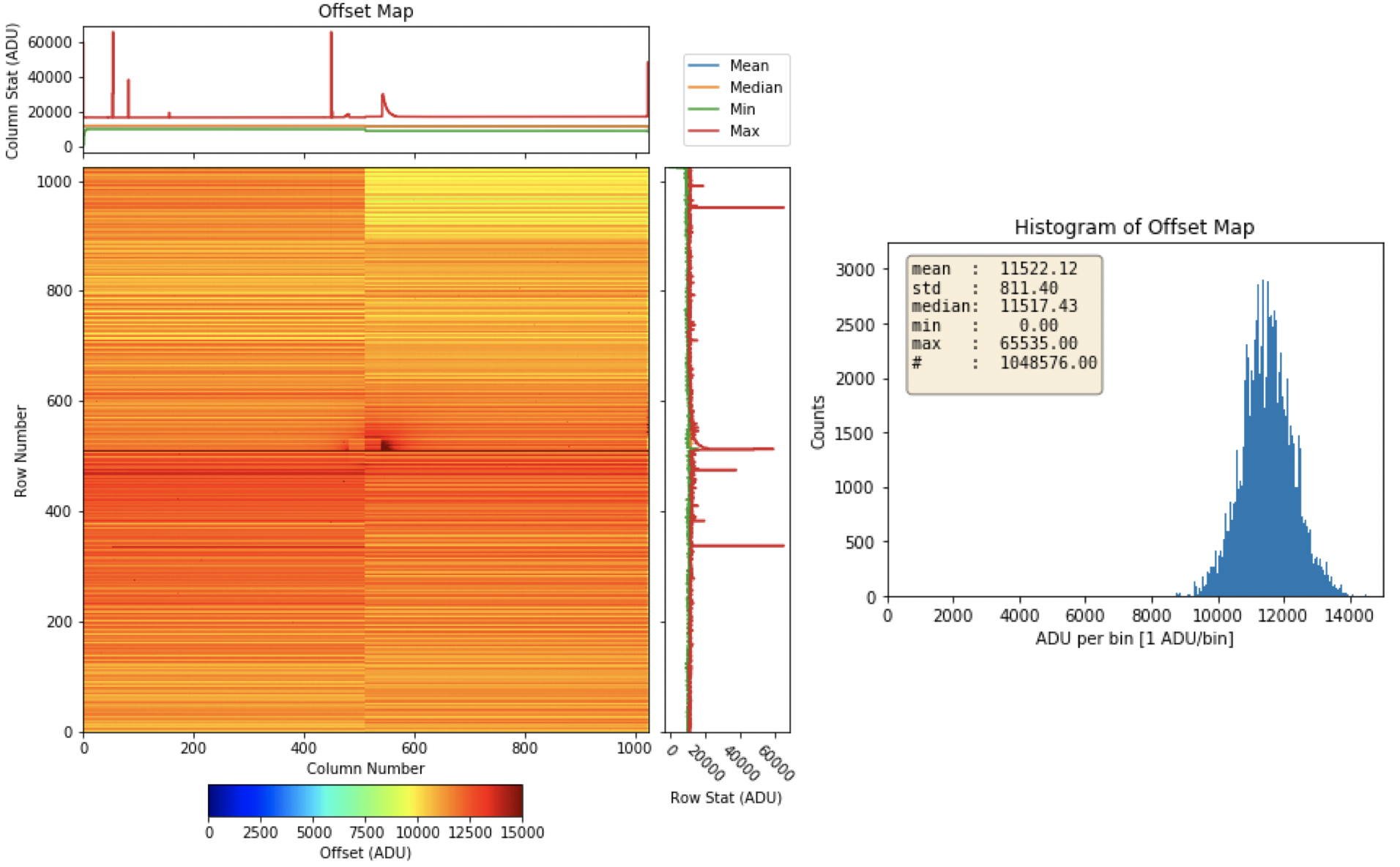
Fig. 3.5 (Right) Offset map, and (left) histogram of the offset map for HDR mode of operation with bias voltage of \(- 470\) V and gain configuration of 1/1. Data are from run 99 in proposal 2720.
Regardless of the bias voltage, the mean offset value calculated across the whole chip slightly decreases with decreasing gain factor until gain 1/64 and then it seems to remian more or less constant in lower gains (see Fig. 3.6). Similarly, the standard deviation in the dark offset decreases with decreasing gain factor until gain 1/16 and then it seems to remian more or less constant in lower gains (see Fig. 3.7).
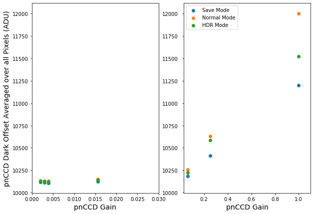
Fig. 3.6 The distribution of pnCCD dark offset (averaged over all pixels) as a function of pnCCD gain.
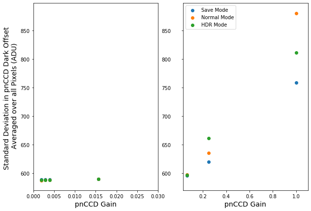
Fig. 3.7 The distribution of the standard deviation in the pnCCD dark offset (averaged over all pixels) as a function of pnCCD gain.
The pnCCD dark offset increases as the detector’s power output increases. The latter is the highest for normal mode of operation (see NormalMode) followed by the HDR mode (see HDRMode) and finally the save mode of operation (see SaveMode).
In some runs, a periodic signal is superimposed on top of the measured dark signal. See CommonMode for a more detailed discussion about this effect.
3.3.4. Offset Stability in Time
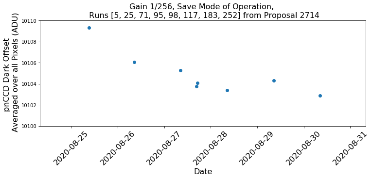
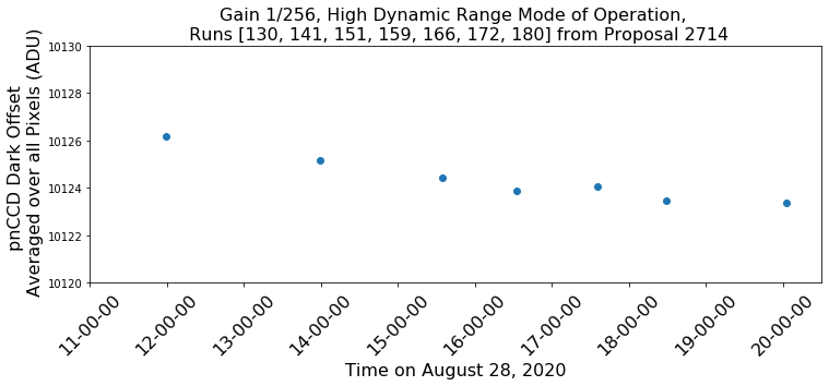
During the first user run with the new pnCCD, the detector was left ON over a few days in the save mode of operation. We power cycled the detector a few times to put it in HDR mode. However, with the dark runs obtained in save mode, we can still study the stability of dark offset as a function of time. Fig. 3.8 and Fig. 3.9 show the results of this stability test in save mode of operation for gains 1/1 and 1/256, respectively. Fig. 3.10 shows the stability of dark offset during half a day in HDR mode of operation for gain 1/256.
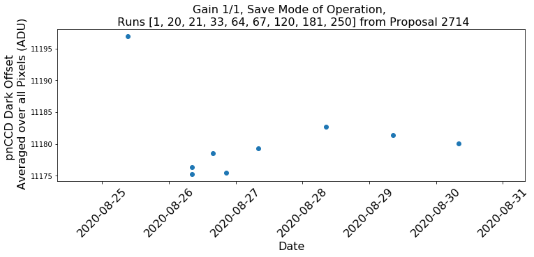
Fig. 3.8 Stability of dark offset (averaged over all pixels) as a function of time for gain 1/1 in save mode of operation. The detector was power cycled before taking runs 64 and 181.
3.3.5. Offset Correction
To correct for the offset, one simply has to subtract the offset map from each individual illuminated image frame.
3.4. Common Mode
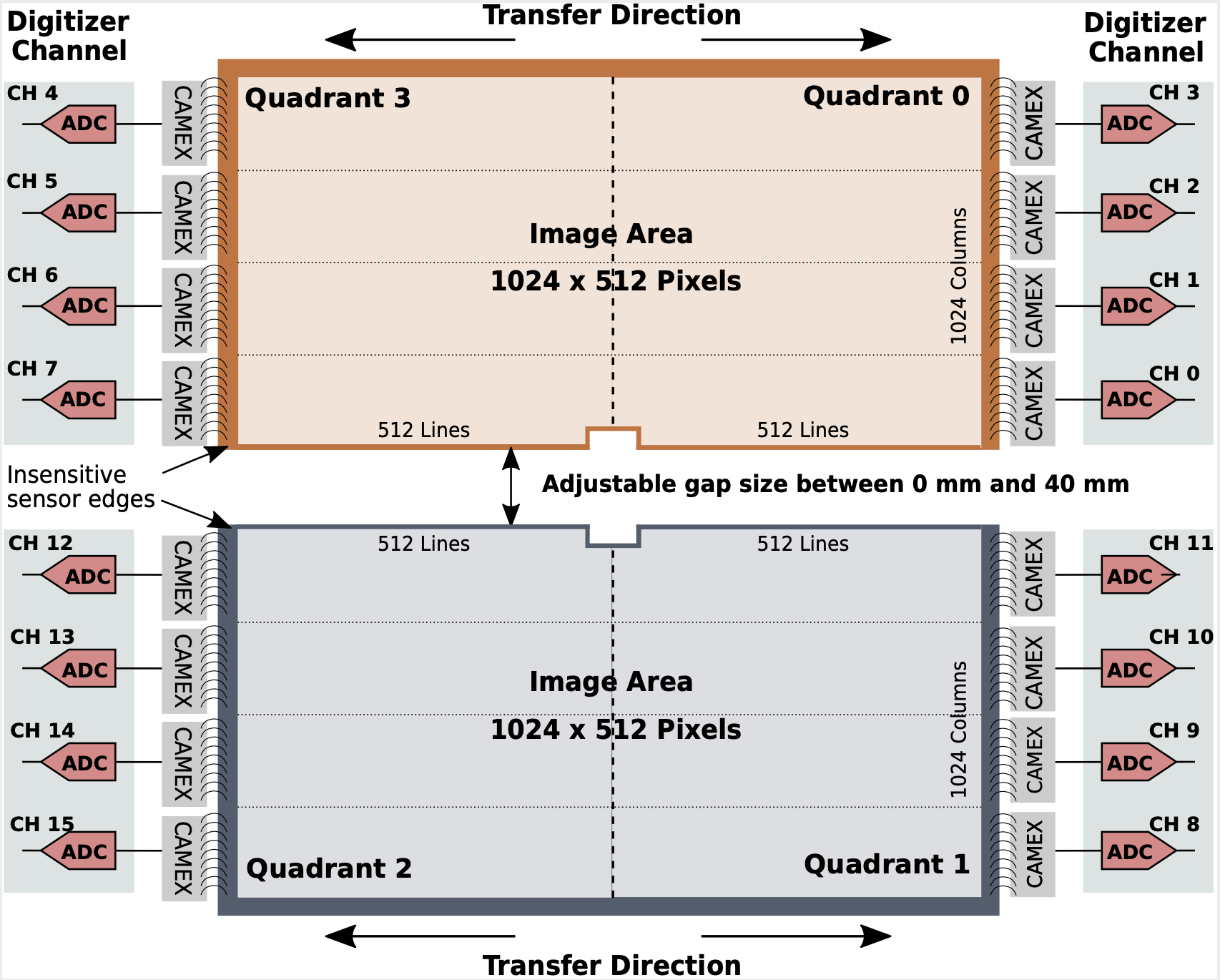
In the pnCCD, every 128 rows called CAMEX (see pnCCD Operation Manual) are connected to the same readout electronics. Therefore, every 128 rows share the same amplifier, etc. As a result, any voltage variation in the readout electronics would affect these rows in a similar fashion.
Common mode is a periodic signal that is superimposed on top of the measured dark signal. Its origin comes from the aforementioned voltage variation in the readout electronics that are shared between every 128 rows. The offset maps of pnCCD are modulated with common mode, whose amplitude changes from frame to frame and from column to column. The frequency of this modulation can change from run to run.
pnCCD has 16 CAMEXs which are divided into 4 quadrants. In other words, charge is read out horizontally along the 1024 rows but each row is separated into two halves, and the readouts are located on the left and right sides of the detector. Consequently, every CAMEX consists of 128 rows by 512 columns. The pnCCD quadrants with their readout electronics are displayed in Fig. 3.11.
In order to calculate the common mode (in ADU), a few factors need to be considered:
- A common mode axis should be determined depending on the readout axis. Common mode axis should always be prependicular to the readout axis for a CCD analysis. This is because in each CCD, a certain number of row (column) readouts share the same readout electronics and they are all going to be affected similarly by the common mode. Therefore, to calculate and correct the common mode effect, one needs a snapshot of pixels that are read out in parallel (at the same time). In other words, one needs to look at the pixels that are being read out at the same time with the same readout electronics. The axis which provides such a snapshot is prependicular to the readout axis.
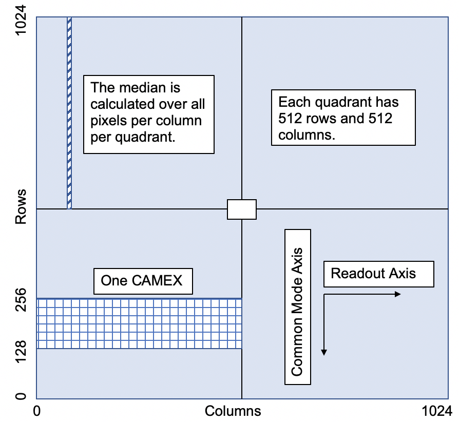
Fig. 3.12 Common mode value (in ADU) is calculated for each image frame. Each image is devided into 4 quadrants consisting of 512 rows by 512 columns. A median of pixel signals is then calculated for all pixels per column, i.e., pixels whose column number is the same (see the hatched area). This is because the readout axis in pnCCD is horizontal, and therefore, the pixels per column are read out at the same time. To correct for common mode, each median value (in ADU) is then subtracted from all pixel signals in the corresponding column, i.e., the subtraction takes place for pixels whose column number is the same. Therefore, 512 median values (corresponding to 512 columns) per quadrant are calculated and each of them is subtracted from all 512 pixels in each corresponding column.
A common mode block size must be determined depending on how many readout rows (columns) in the CCD share the same electronics. For example, in pnCCD, a CAMEX is defined to be every 128 rows, which share the same readout electronics (see the grid area in Fig. 3.12). In each row, there are 512 pixels (corresponding to 512 columns in that quadrant). Therefore, a CAMEX is the ideal common mode block size for pnCCD.
Depending on the readout structure, it may be the case that every \(n\) row (column) readout in a CCD shows a strong correlation due to the common mode effect. Generally, such correlations should be studied in advance to the common mode calculation. To correct for this effect, a median of the pixel signals shall be calculated over every \(n\) pixels along the common mode axis. Finally, this median should be subtracted from all pixels along the common mode axis to remove these correlations. In the CCD notebooks developed at European XFEL, we have attributed a variable called stride for the definition of common mode. Stride is the same as \(n\) in the desription above. Thus, if stride \(= 10\), this means that the median is calculated taking into account the pixel signals of every 10 pixels along the common mode axis. This median is then subtracted from pixel signals of all pixels along the common mode axis.
To acurately calculate the common mode effect, one needs to use pixels with reasonable event statistics. A variable called
minFracis defined, which is the minimum acceptable fractional number of pixels that can be evaluated for common mode calculation.minFracparameter is used to reject common mode values calculated with too few pixels without events. A pixel is rejected from evaluation of common mode if:- it is marked in the bad pixel map (see
BadPixels). - its signal value (in ADU) is larger than 4 times the value of noise (in ADU) of that pixel, i.e., there is an event in that pixel for that frame.
- it is marked in the bad pixel map (see
If the number of usable (not rejected) pixels in a row (column) of \(N\) pixels is less than minFrac \(\times\) \(N\), the common mode is set to 0, i.e., it is not evaluated from that row (column). This is to prevent areas of the sensor with larger event numbers that skew the common mode distribution significantly. In other words, common mode correction is only considered sensible for sparse datasets. Because minFrac denotes the minimum fraction of usable pixels with respect to all pixels, it should have a value between 0 and 1. minFrac \(=\) 0 means that the common mode is evaluated for all rows (columns), depending on the common mode axis, except those that have NaN values due to the presence of bad pixels in that row (column). Only those rows (columns) are ignored in this case.
To acquire the common mode values (in ADU) for pnCCD, the following calculation is performed per image frame:
- The image frame is first devided into 4 quadrants each having 512 rows by 512 columns (see Fig. 3.12).
- Since the readout axis for pnCCD is horizontal (along the rows), the common mode axis must be vertical (along the columns). This is shown by the hatched area on Fig. 3.12.
- The common mode block size for pnCCD analysis is not defined to be the size of a CAMEX (128 rows by 512 columns). To increase the likelihood of having enough pixels without high intensity events to be used for common mode calculation, Robert Hartmann from the PNSensor company suggested to use the pnCCD quadrant as the common mode block size. This means that the block size is defined to be 512 rows by 512 columns.
- For pnCCD, we let stride (see above) be equal to 1, which means the median is calculated over all pixels along the common mode axis, i.e., no pixel is skipped.
- The
minFracparameter is set to \(0\) for dark runs. This was chosen after analyzing many dark runs with different operation modes and gains. Since the pnCCD detector is new and it does not have any permanently bad pixels, dark runs usually do not show a high percentage of bad pixels. Therefore, if a run is dark, we would use all pixels in each column for calculation of common mode. Of course, those columns that may have a bad pixel in them are ignored, and common mode is not evaluated for them as described previously. On the other hand, if a run is not dark and contains illuminated data, theminFracparameter is set to \(0.25\). This means that the number of usable pixels per column must be at least 128 in order to evaluate the common mode from that column.- Finally, per quadrant, a median of pixel signal is calculated for all 512 pixels per column, i.e., pixels whose column number is the same (see the hatched area in Fig. 3.12).
- Therefore, per quadrant 512 common mode values (in ADU) corresponding to 512 columns in that quadrant are obtained. Each of these values is the common mode for one of the columns in that quadrant.
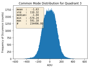
Fig. 3.13 For quadrant 3. |
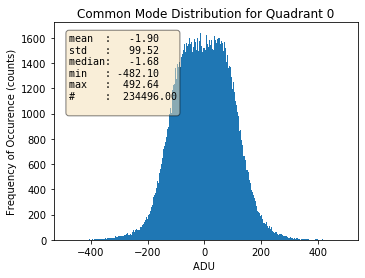
Fig. 3.14 For quadrant 0. |
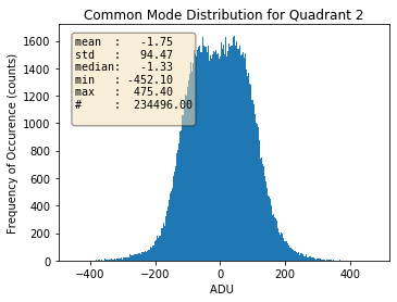
Fig. 3.15 For quadrant 2. |
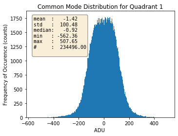
Fig. 3.16 For quadrant 1. |
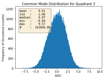
Fig. 3.17 Ffor quadrant 3. |
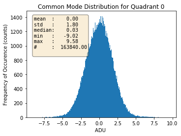
Fig. 3.18 For quadrant 0. |
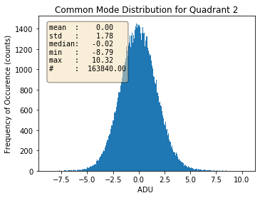
Fig. 3.19 For quadrant 2. |
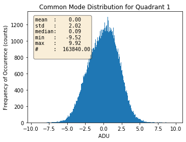
Fig. 3.20 For quadrant 1. |
Histograms of the calculated common modes per column per quadrant for gain 1/1 are shown in Table 3.4 for normal mode of operation of pnCCD as an example. Prior to calculation of these common mode values, the dark data were already corrected for the offset. This is why these histograms are centered near zero.
With decreasing the gain factor (gains \(=\) 1/16, 1/64, 1/256, 1/340 and 1/512), these distributions get much narrower (with reduced standard deviations) and get more centered around zero (see Table 3.5). This may be due to the fact that the noise is dominated by the electronics for these gains. However, the distributions are not always Gaussian, particularly for quadrants 1 and 3 (see Table 3.5).
Fig. 3.21 shows, as an example, the common mode values per column versus column numbers for each pnCCD quadrant corresponding to gain 1/340 in HDR mode of operation. This plot is only the snapshot of a particular image frame, namely frame 245. The modulation of the baseline dark signal is rather obvious for this example. In contrast, Fig. 3.22 shows the same results but for a dark run with gain 1/1 in save mode of operation. It looks like the modulation of the baseline dark signal is not too much for the latter example.
Common mode distribution changes from frame to frame, from column to column and from run to run (see Fig. 3.23).
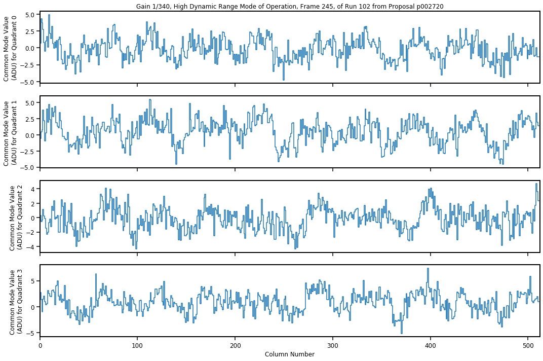
Fig. 3.21 Common mode values (in ADU) calculated per column versus the column number (related to time, see FourierTransform) for each pnCCD quadrant is shown for the image frame 245 of dark run number 102 proposal 2720. Gain was set to 1/340. pnCCD was in HDR mode of operation. This run has a total of 311 acquired frames. The modulation of the baseline signal is visible for all quadrants.
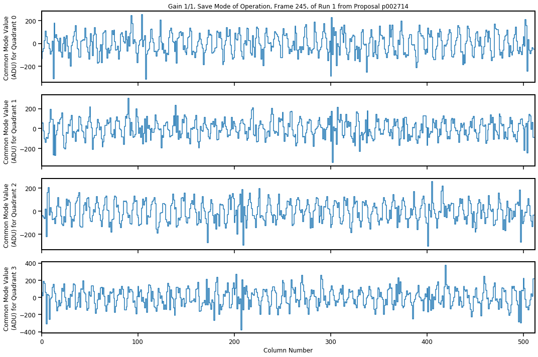
Fig. 3.22 Common mode values (in ADU) calculated per column versus the column number (related to time, see FourierTransform) for each pnCCD quadrant is shown for the image frame 245 of dark run number 1 proposal 2714. Gain was set to 1/1 and pnCCD was in save mode of operation. This run has a total of 482 acquired frames. The modulation of the baseline signal is negligible for all quadrants.
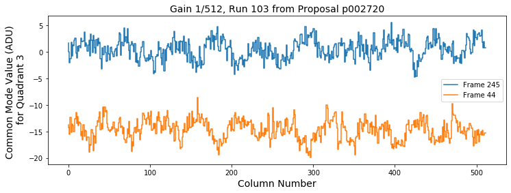
Fig. 3.23 Common mode values (in ADU) calculated per column versus the column number for pnCCD quadrant 3 is shown for the two image frames of dark run number 103 proposal 2720. Gain was set to 1/512 and pnCCD was in HDR mode of operation. The results for frame 44 are shifted downwards by 15 ADU for visibility of both plots.
3.4.1. Common Mode Distribution
A Fourier transform of the time domain of the common mode values per quadrant will provide us with the frequencies at which common mode is observed. To obtain these frequencies, we first need to acquire the time domain of the common mode values per quadrant.
Time (in \(\mu\!\) s) to read a row per pnCCD quadrant is equal to:
where 512 is the number of pixels in a row per quadrant, and \(t\) is the time to read one pixel in the readout axis. The latter is determined by the pixel clock set by PNSensor. This is currently set to 29.2 \(\mu\!\) s, which is the time to read column-by-column pixels. Note that all rows in a quadrant are read out in parallel (at the same time). The pnCCD readout clock runs at 10 Hz. In other words, frame rate is 10 Hz given by FEL timing generator. Therefore, there is 100 ms (or 100000 \(\mu\!\) s) time between two successive images. It follows that the time (in \(\mu\!\) s) between when all rows (readout axes) per quadrant are fully read and when the next X-ray pulse hits the detector producing the next image frame will be:
where 512 is the number of pixels in a row per quadrant. Assuming that the first time-array corresponds to all rows per quadrant (each row consists of 512 columns, and all rows are read out in parallel at the same time meaning that pixels with the same position in all rows are being read out with identical timing) in an image, the next time-array (corresponding to the next image) should be concatenated to the first time-array with a 85049.6 \(\mu\!\) s gap in between the two time arrays. Also, the duration of each image should be 100 ms. If we then make a 1D time-array of all images per quadrant this way, we will have the time axis. The y-axis would contain the common mode values (in ADU) corresponding to each quadrant per image. If we plot y-axis vs. time, we will obtain the time domain of common mode values per quadrant. If we then make a Fourier transform of this distribution, we should see the frequencies of parasitic signals caused by the common mode.
It is worthwhile to mention that according to Robert Hartmann:
- Within 29.2 \(\mu\!\) s, the signals of all 128 channnels of one CAMEX are readout with a frequency of 200 ns. This is the frequency which we use as the sampling rate for our Fourier transform .
- The readout of one column takes 25.6 \(\mu\!\) s and there is \(29.2 - 25.6 = 3.6\) \(\mu\!\) s delay before the next column.
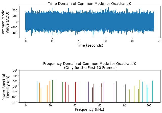
Two examples of the time and frequency distributions of the common mode for pnCCD quadrant 0 are shown in Fig. 3.24 for only the first frame, and in Fig. 3.25 for the first 10 image frames observed in that run. These examples are for gain 1/1 in save mode of operation. Fig. 3.26 shows the Power Spectral Density (PSD) for the first 10 image frames in the same run. PSD is the measure of common mode signals’ power content versus frequency.
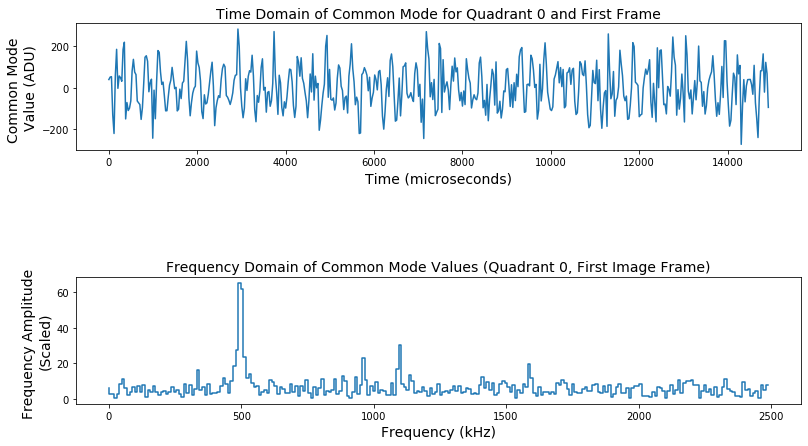
Fig. 3.24 Common mode time and frequency distributions obtained for the first image frame in quadrant 0 of pnCCD. Gain was set to 1/1, and the detector was operating in save mode of operation. Data are from dark run number 1 in proposal 2714. The time for acquiring one image frame is 512 \(\times\) 29.2 \(\mu\!\) s, where 512 is the number of pixels in a readout axis and 29.2 \(\mu\!\) s is the time to read one column in the readout axis, i.e., one pixel.
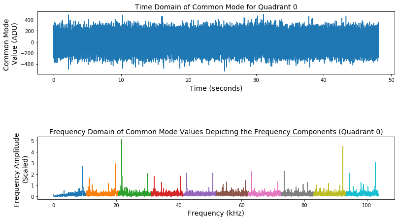
Fig. 3.25 Common mode time and frequency distributions obtained for the first 10 image frames saved in the run. Each image frame is shown using a different color. This plot is only for quadrant 0 of pnCCD. Gain was set to 1/1, and the detector was operating in save mode of operation. Data are from dark run number 1 in proposal 2714. Here, the time includes the 85049.6 \(\mu\!\) s gaps in between the two successive image frames. Clearly, there are two frequencies that show up in each image frame with identical intervals. These are two peaks towards the beginning and end of each color band, and they may refer to the two clocks that keep repeating (29.2 \(\mu\!\) s and 85049.6 \(\mu\!\) s). The frequency amplitudes are normalized to the number of frequencies in the calculated frequency array.
3.4.2. Common Mode Correction
To correct for common mode effect, each of the 512 common mode values (in ADU) per quadrant are subtracted from the pixel signals (in ADU) for all pixels of the corresponding column, i.e., pixels whose column number is the same. Such a common mode correction applied per quadrant yields the best results in terms of homogeneity.
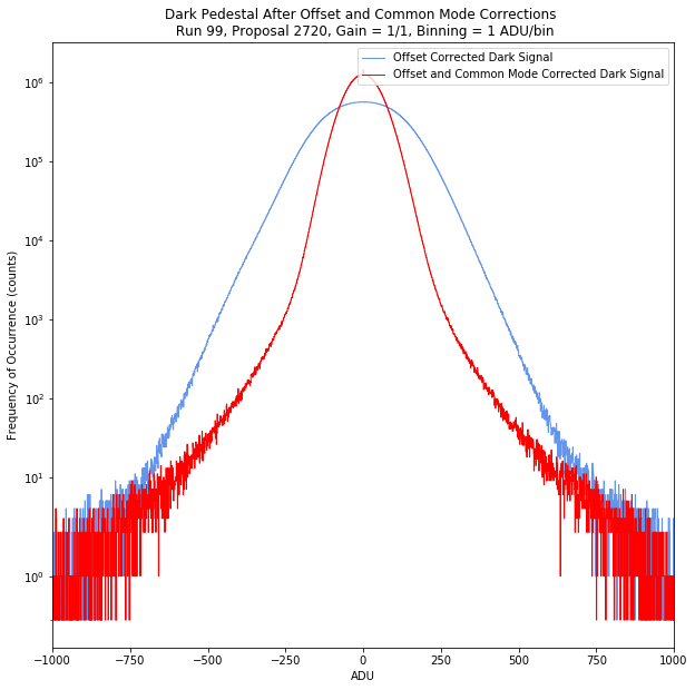
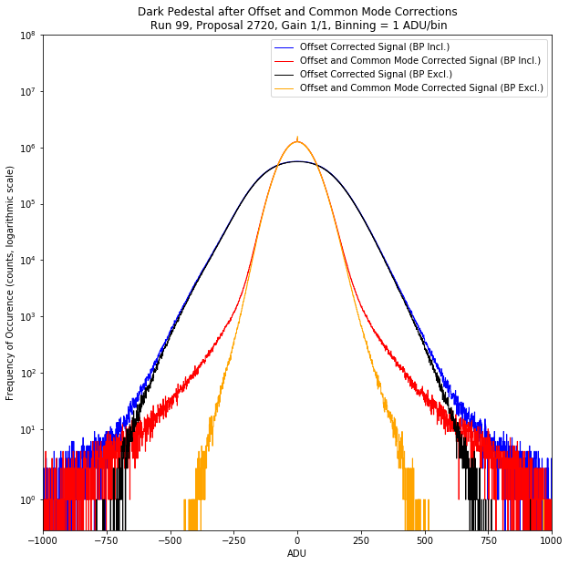
Correcting the common mode effect reduces the detector noise. Before going into a detailed discussion on noise (see Noise), it is worthwhile to mention that at high gains such as 1/1 and 1/4, the noise is entirely dominated by the CCD detector noise. Whereas, at lower gains (1/16, 1/64, 1/256, 1/340 and 1/512), the noise is dominated by the electronics noise coming from the FastADCs, etc. Table 3.6 shows an example of histograms of offset corrected dark signals prior to and after common mode correction for gain 1/1. An offset corrected dark signal shlould ideally be centered at zero. When we have common mode correction in addition to the offset correction, the full width at half maximum of the corrected signal is much reduced, which means the noise is reduced, and the result has a median that is more centered around zero as shown in Table 3.6.

|
|
3.5. Noise
As a crude estimation, the uncorrected noise map is a matrix of 1024 \(\times\) 1024 pixels whose values (in ADU) correspond to:
where \(N\) is the total number of frames acquired in the dark run, \(Signal\) is the value (in ADU) for each pixel of the pnCCD detector, and \(\mu\) is the dark offset value (in ADU) for the same pixel from the offset map, i.e., \(\mu\) is the mean (over all frames) of dark signal per pixel, which is the dark offset. Therefore, the uncorrected noise map is the standard deviation (over the total available trains or frames) from the dark offset per pixel.
The above description is only a crude estimation of the actual noise. Fig. 3.27 and Fig. 3.28 show examples of such an uncorrected noise map.
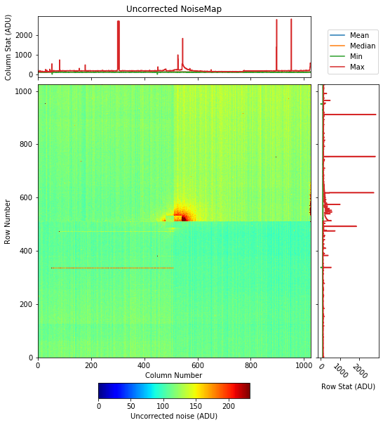
Fig. 3.27 The uncorrected noise map essentially shows the standard deviation (over all image frames) in the dark offset per pixel. Data are from run 99 in proposal 2720. Gain was set to 1/1 and, the pnCCD was in HDR mode of operation.
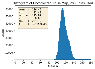
Fig. 3.28 Histogram of the uncorrected noise map. Data are from run 99 in proposal 2720. Gain was set to 1/1 and, the pnCCD was in HDR mode of operation.
3.5.1. Effect of Common Mode Correction on the Noise Level
A better estimation of the noise is achieved by correcting the dark data for offset (see OffsetCorrection) and common mode (see CommonModeCorrection).
Calculating the standard deviation of the offset and common mode corrected dark signal results in the first good estimate of the noise map. In other words, the noise map depicts standard deviation of the offset and common mode corrected dark signal per pixel, where the standard deviation is taken over the number of available image frames. Fig. 3.29 and Fig. 3.30 show examples of such a corrected noise map.
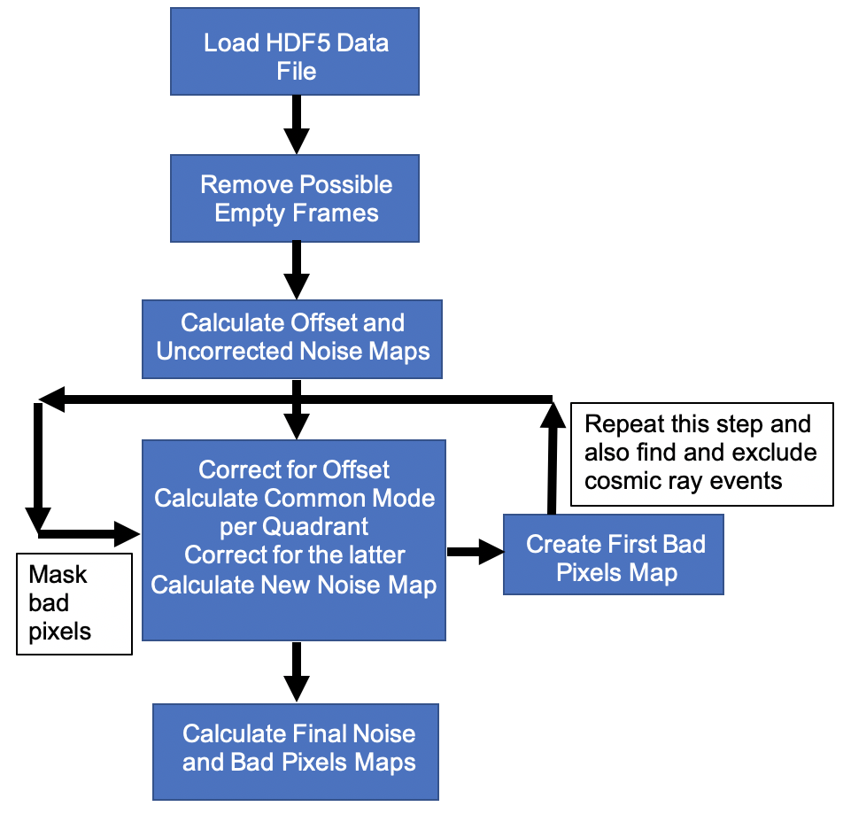
From this noise map, one can identify the noisy pixels (see BadPixels). Applying a mask on these bad pixels, the procedure of correcting the dark signal for offset, and common mode is repeated once again after masking the bad pixels. In addition, one can search for and exclude the cosmic ray events. Eventually, by calculating the standard deviation (over all image frames) of the final offset and common mode corrected dark signal, the final noise map is obtained. Fig. 3.31 shows the algorithm to obtain the final noise map, and Fig. 3.35 and Fig. 3.36 show examples of the final noise map with all bad pixels excluded.
Table 3.7 summarizes the final noise (averaged over all pixels) accross the entire detector for different gain and bias voltage configurations. Table 3.8 summarizes the average (over all pixels per quadrant) final noise for the individual pnCCD quadrants for different gain and bias voltage configurations.
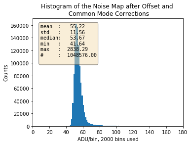
Fig. 3.29 Histogram of the noise map after applying offset and common mode corrections to the dark data. The standard deviation of the distribution is greatly reduced (in comparison with Fig. 3.28) due to the corrections. Data are from run 99 in proposal 2720. Gain was set to 1/1 and, the pnCCD was in HDR mode of operation.
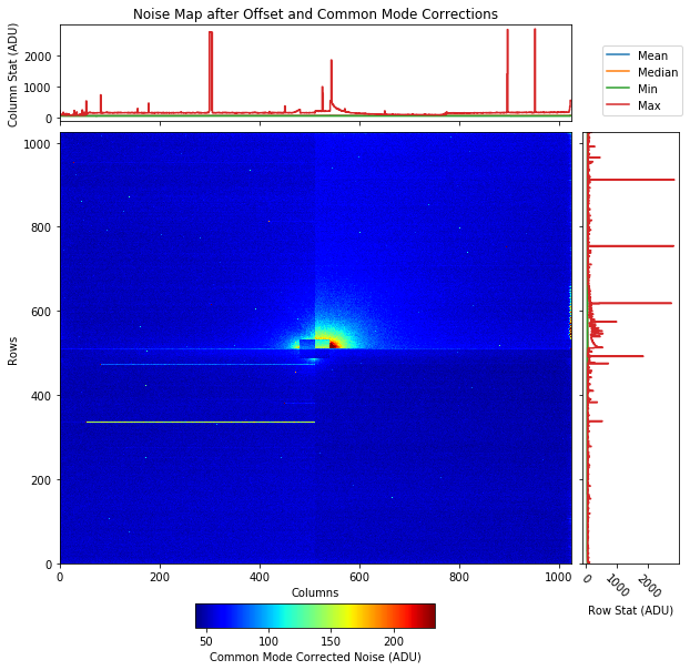
Fig. 3.30 After correcting the dark offset and performing a common mode correction on the offset corrected data, we obtain this noise map, which shows the standard deviation (over all image frames) in the corrected dark signal per pixel. Bad pixels are still included. This noise map is a better estimation of the actual noise. Data are from run 99 in proposal 2720. Gain was set to 1/1 and, the pnCCD was in HDR mode of operation.
| pnCCD Gain | Uncorrected Noise | Corrected Noise (Bad Pixels Included) | Corrected Noise (Bad Pixels Excluded) | Operation Mode |
| 1/1 | 140 \(\pm\) 20 ADU | 95 \(\pm\) 23 ADU | 94 \(\pm\) 19 ADU | Normal |
| 1/4 | 36 \(\pm\) 15 ADU | 26 \(\pm\) 15 ADU | 25 \(\pm\) 5 ADU | Normal |
| 1/16 | 13 \(\pm\) 2 ADU | 11 \(\pm\) 2 ADU | 10.62 \(\pm\) 0.99 ADU | Normal |
| 1/64 | 9 \(\pm\) 1 ADU | 8.7 \(\pm\) 1.0 ADU | 8.7 \(\pm\) 0.5 ADU | Normal |
| 1/256 | 8.8 \(\pm\) 0.4 ADU | 8.6 \(\pm\) 0.4 ADU | 8.6 \(\pm\) 0.34 ADU | Normal |
| 1/340 | 8.7 \(\pm\) 0.4 ADU | 8.5 \(\pm\) 0.3 ADU | 8.4 \(\pm\) 0.5 ADU | Normal |
| 1/512 | 8.6 \(\pm\) 0.3 ADU | 8.4 \(\pm\) 0.3 ADU | 8.3 \(\pm\) 0.5 ADU | Normal |
| 1/1 | 116 \(\pm\) 12 ADU | 55 \(\pm\) 11 ADU | 55 \(\pm\) 6 ADU | High Dynamic Range |
| 1/4 | 34 \(\pm\) 9 ADU | 21 \(\pm\) 10 ADU | 21 \(\pm\) 6 ADU | High Dynamic Range |
| 1/16 | 12 \(\pm\) 4 ADU | 9 \(\pm\) 3 ADU | 9.3 \(\pm\) 0.7 ADU | High Dynamic Range |
| 1/64 | 9.0 \(\pm\) 0.5 ADU | 8.6 \(\pm\) 0.4 ADU | 8.62 \(\pm\) 0.38 ADU | High Dynamic Range |
| 1/256 | 8.7 \(\pm\) 0.4 ADU | 8.5 \(\pm\) 0.4 ADU | 8.54 \(\pm\) 0.37 ADU | High Dynamic Range |
| 1/340 | 8.6 \(\pm\) 0.4 ADU | 8.4 \(\pm\) 0.4 ADU | 8.45 \(\pm\) 0.37 ADU | High Dynamic Range |
| 1/512 | 8.6 \(\pm\) 0.4 ADU | 8.3 \(\pm\) 0.4 ADU | 8.34 \(\pm\) 0.37 ADU | High Dynamic Range |
| 1/1 | 111 \(\pm\) 13 ADU | 48 \(\pm\) 12 ADU | 47 \(\pm\) 8 ADU | Save |
| 1/4 | 29 \(\pm\) 9 ADU | 14 \(\pm\) 9 ADU | 14 \(\pm\) 1 ADU | Save |
| 1/16 | 11 \(\pm\) 2 ADU | 8.9 \(\pm\) 1.7 ADU | 8.8 \(\pm\) 0.6 ADU | Save |
| 1/64 | 8.8 \(\pm\) 1.1 ADU | 8.4 \(\pm\) 1.1 ADU | 8.4 \(\pm\) 0.5 ADU | Save |
| 1/256 | 8.6 \(\pm\) 0.4 ADU | 8.3 \(\pm\) 0.4 ADU | 8.3 \(\pm\) 0.5 ADU | Save |
| 1/340 | 8.5 \(\pm\) 0.3 ADU | 8.3 \(\pm\) 0.3 ADU | 8.2 \(\pm\) 0.5 ADU | Save |
| 1/512 | 8.4 \(\pm\) 0.3 ADU | 8.2 \(\pm\) 0.3 ADU | 8.1 \(\pm\) 0.5 ADU | Save |
| pnCCD Gain | pnCCD Quadrant | Final Noise | Operation Mode | Run/Proposal |
| 1/1 | Lower Left Quadrant | 48 \(\pm\) 2 ADU | Save | 1 / 2714 |
| Upper Left Quadrant | 48 \(\pm\) 2 ADU | |||
| Lower Right Quadrant | 49 \(\pm\) 2 ADU | |||
| Upper Right Quadrant | 46 \(\pm\) 2 ADU | |||
| 1/4 | Lower Left Quadrant | 14 \(\pm\) 1 ADU | Save | 2 / 2714 |
| Upper Left Quadrant | 14 \(\pm\) 1 ADU | |||
| Lower Right Quadrant | 15 \(\pm\) 1 ADU | |||
| Upper Right Quadrant | 14 \(\pm\) 1 ADU | |||
| 1/16 | Lower Left Quadrant | 8.8 \(\pm\) 0.4 ADU | Save | 3 / 2714 |
| Upper Left Quadrant | 8.9 \(\pm\) 0.3 ADU | |||
| Lower Right Quadrant | 9.1 \(\pm\) 0.3 ADU | |||
| Upper Right Quadrant | 8.8 \(\pm\) 0.3 ADU | |||
| 1/64 | Lower Left Quadrant | 8.4 \(\pm\) 0.3 ADU | Save | 4 / 2714 |
| Upper Left Quadrant | 8.4 \(\pm\) 0.3 ADU | |||
| Lower Right Quadrant | 8.6 \(\pm\) 0.3 ADU | |||
| Upper Right Quadrant | 8.3 \(\pm\) 0.3 ADU | |||
| 1/256 | Lower Left Quadrant | 8.3 \(\pm\) 0.4 ADU | Save | 5 / 2714 |
| Upper Left Quadrant | 8.3 \(\pm\) 0.3 ADU | |||
| Lower Right Quadrant | 8.5 \(\pm\) 0.4 ADU | |||
| Upper Right Quadrant | 8.3 \(\pm\) 0.3 ADU | |||
| 1/340 | Lower Left Quadrant | 8.2 \(\pm\) 0.3 ADU | Save | 6 / 2714 |
| Upper Left Quadrant | 8.2 \(\pm\) 0.3 ADU | |||
| Lower Right Quadrant | 8.4 \(\pm\) 0.3 ADU | |||
| Upper Right Quadrant | 8.2 \(\pm\) 0.3 ADU | |||
| 1/512 | Lower Left Quadrant | 8.1 \(\pm\) 0.3 ADU | Save | 7 / 2714 |
| Upper Left Quadrant | 8.1 \(\pm\) 0.3 ADU | |||
| Lower Right Quadrant | 8.4 \(\pm\) 0.3 ADU | |||
| Upper Right Quadrant | 8.1 \(\pm\) 0.3 ADU | |||
| 1/1 | Lower Left Quadrant | 81 \(\pm\) 13 ADU | Normal | 338 / 900166 |
| Upper Left Quadrant | 110 \(\pm\) 15 ADU | |||
| Lower Right Quadrant | 89 \(\pm\) 12 ADU | |||
| Upper Right Quadrant | 100 \(\pm\) 15 ADU | |||
| 1/4 | Lower Left Quadrant | 22 \(\pm\) 3 ADU | Normal | 339 / 900166 |
| Upper Left Quadrant | 29 \(\pm\) 4 ADU | |||
| Lower Right Quadrant | 24 \(\pm\) 3 ADU | |||
| Upper Right Quadrant | 27 \(\pm\) 4 ADU | |||
| 1/16 | Lower Left Quadrant | 10 \(\pm\) 1 ADU | Normal | 340 / 900166 |
| Upper Left Quadrant | 11 \(\pm\) 1 ADU | |||
| Lower Right Quadrant | 11 \(\pm\) 1 ADU | |||
| Upper Right Quadrant | 11 \(\pm\) 1 ADU | |||
| 1/64 | Lower Left Quadrant | 8.6 \(\pm\) 0.3 ADU | Normal | 341 / 900166 |
| Upper Left Quadrant | 8.8 \(\pm\) 0.3 ADU | |||
| Lower Right Quadrant | 8.9 \(\pm\) 0.3 ADU | |||
| Upper Right Quadrant | 8.6 \(\pm\) 0.3 ADU | |||
| 1/256 | Lower Left Quadrant | 8.6 \(\pm\) 0.3 ADU | Normal | 342 / 900166 |
| Upper Left Quadrant | 8.6 \(\pm\) 0.3 ADU | |||
| Lower Right Quadrant | 8.8 \(\pm\) 0.3 ADU | |||
| Upper Right Quadrant | 8.5 \(\pm\) 0.3 ADU | |||
| 1/340 | Lower Left Quadrant | 8.4 \(\pm\) 0.3 ADU | Normal | 343 / 900166 |
| Upper Left Quadrant | 8.5 \(\pm\) 0.3 ADU | |||
| Lower Right Quadrant | 8.7 \(\pm\) 0.3 ADU | |||
| Upper Right Quadrant | 8.3 \(\pm\) 0.3 ADU | |||
| 1/512 | Lower Left Quadrant | 8.3 \(\pm\) 0.3 ADU | Normal | 344 / 900166 |
| Upper Left Quadrant | 8.4 \(\pm\) 0.3 ADU | |||
| Lower Right Quadrant | 8.6 \(\pm\) 0.3 ADU | |||
| Upper Right Quadrant | 8.2 \(\pm\) 0.3 ADU | |||
| 1/1 | Lower Left Quadrant | 55 \(\pm\) 5 ADU | High Dynamic Range | 99 / 2720 |
| Upper Left Quadrant | 53 \(\pm\) 3 ADU | |||
| Lower Right Quadrant | 59 \(\pm\) 7 ADU | |||
| Upper Right Quadrant | 51 \(\pm\) 3 ADU | |||
| 1/4 | Lower Left Quadrant | 25 \(\pm\) 6 ADU | High Dynamic Range | 127 / 2714 |
| Upper Left Quadrant | 17 \(\pm\) 3 ADU | |||
| Lower Right Quadrant | 25 \(\pm\) 5 ADU | |||
| Upper Right Quadrant | 16 \(\pm\) 2 ADU | |||
| 1/16 | Lower Left Quadrant | 9.2 \(\pm\) 0.4 ADU | High Dynamic Range | 104 / 2720 |
| Upper Left Quadrant | 9.2 \(\pm\) 0.4 ADU | |||
| Lower Right Quadrant | 9.6 \(\pm\) 0.7 ADU | |||
| Upper Right Quadrant | 9.1 \(\pm\) 0.4 ADU | |||
| 1/64 | Lower Left Quadrant | 8.5 \(\pm\) 0.4 ADU | High Dynamic Range | 100 / 2720 |
| Upper Left Quadrant | 8.6 \(\pm\) 0.4 ADU | |||
| Lower Right Quadrant | 8.8 \(\pm\) 0.4 ADU | |||
| Upper Right Quadrant | 8.5 \(\pm\) 0.4 ADU | |||
| 1/256 | Lower Left Quadrant | 8.5 \(\pm\) 0.4 ADU | High Dynamic Range | 101 / 2720 |
| Upper Left Quadrant | 8.5 \(\pm\) 0.4 ADU | |||
| Lower Right Quadrant | 8.7 \(\pm\) 0.4 ADU | |||
| Upper Right Quadrant | 8.4 \(\pm\) 0.3 ADU | |||
| 1/340 | Lower Left Quadrant | 8.4 \(\pm\) 0.4 ADU | High Dynamic Range | 102 / 2720 |
| Upper Left Quadrant | 8.4 \(\pm\) 0.4 ADU | |||
| Lower Right Quadrant | 8.6 \(\pm\) 0.4 ADU | |||
| Upper Right Quadrant | 8.4 \(\pm\) 0.3 ADU | |||
| 1/512 | Lower Left Quadrant | 8.3 \(\pm\) 0.3 ADU | High Dynamic Range | 103 / 2720 |
| Upper Left Quadrant | 8.3 \(\pm\) 0.3 ADU | |||
| Lower Right Quadrant | 8.5 \(\pm\) 0.3 ADU | |||
| Upper Right Quadrant | 8.3 \(\pm\) 0.3 ADU |
3.6. Bad Pixels
The bad pixels map provides information about those pixels which should be permanently excluded from the data analysis due to their signal properties. This map is a matrix of 1024 rows by 1024 columns of pixels and is derived from dark data analysis (see Fig. 3.31). The following thresholds are applied frame-by-frame to identify such pixels:
- Offset Threshold: pixels whose signal values (in ADU) are:
where Offset refers to the offset map from dark data, median and standard deviation (\(\sigma\)) of the offset map are calculated over all image frames ignoring all possible NaN (not a number) values, and \(4\sigma_{O}\) refers to 4 times standard deviation of the offset, which is a limit considered at XFEL for CCD analysis based on recommendation from PNSensor company for bad pixels identification. Table 3.1 to Table 3.3 show the means and standard deviations of offset maps calculated per operation mode and pnCCD gain. To estimate signal values corresponding to bad pixels from the above mentioned equation, please use the Offset (BP Incl.) column and keep in mind that those are the mean offset values. Median values are up to 20 ADU higher.
- Noisy Threshold: Similarly, noisy pixels are those for which the rms noise of a pixel is:
where Noise refers to the rms noise map from dark data calculated accross the whole detector, and \(\sigma_{N}\) is the standard deviation of the rms noise. This is the final noise map after offset and common mode corrections are applied to the data. The areas/pixels identified by the above procedure, should be marked in the bad pixels map and are excluded from the data analysis.
- If there are possible cosmic ray events registered by the detector while taking data, the pixels whose signal values correspond to these events are identified and masked. These pixels are also marked in the bad pixels map and are excluded from the data analysis. The identification of cosmic ray events takes place by finding pixels whose signal values are:
where Signal is the offset and common mode corrected pixel-signal (in ADU), and Noise is the final rms noise map from dark data calculated accross the whole detector after offset and common mode corrections are applied to the data.
- Pixels in the central rectangular hole area of the pnCCD are also marked in the bad pixels map and are excluded from the data analysis. According to PNSensor, each pnCCD sensor (top and bottom detectors) has 22 rows and 60 columns cut out by a laser. Therefore, the central hole of the pnCCD starts from pixel coordinates \(=\) (489, 481), and ends at pixel coordinates \(=\) (533, 541), where the numbers in each parentheses set are the row and column numbers, respectively. The indices for counting rows and columns start from zero. This area is masked and is added to the bad pixels map.
- The edge pixels: according to PNSensor, the pixels on the first and last row and the first and last column should be marked as bad pixels and be excluded from the data analysis.
The number of bad pixels marked on the bad pixels map changes significantly from run to run and between different gain, bias voltage and X-ray intensity configurations. This effect can be mostly attributed to changing experiment and detector operating conditions. The bad pixels map is not static, i.e., each dark run results in a separate independent bad pixels map. The total number of bad pixles is at best around \(0.3\%\) of the entire number of pnCCD pixels and at worse may be well below \(5\%\) of the total number of pnCCD pixels. Table 3.9 shows an example of a bad pixels map acquired during commissioning of pnCCD in August 2020.
3.6.1. Effect of Bad Pixels on Offset Map and Noise Map
As mentioned before, normally the elimination of all bad pixels (see BadPixels) does not affect the offset map so much (see for example offsetSection). Masking bad pixels would of course reduce the standard deviation in the dark offset and possibly move its mean (over all pixels) to a lower value by a few ADU. Fig. 3.33 shows an example of statistics on the offset map with and without the bad pixels. Fig. 3.34 shows an example of the offset maps with and without bad pixels.
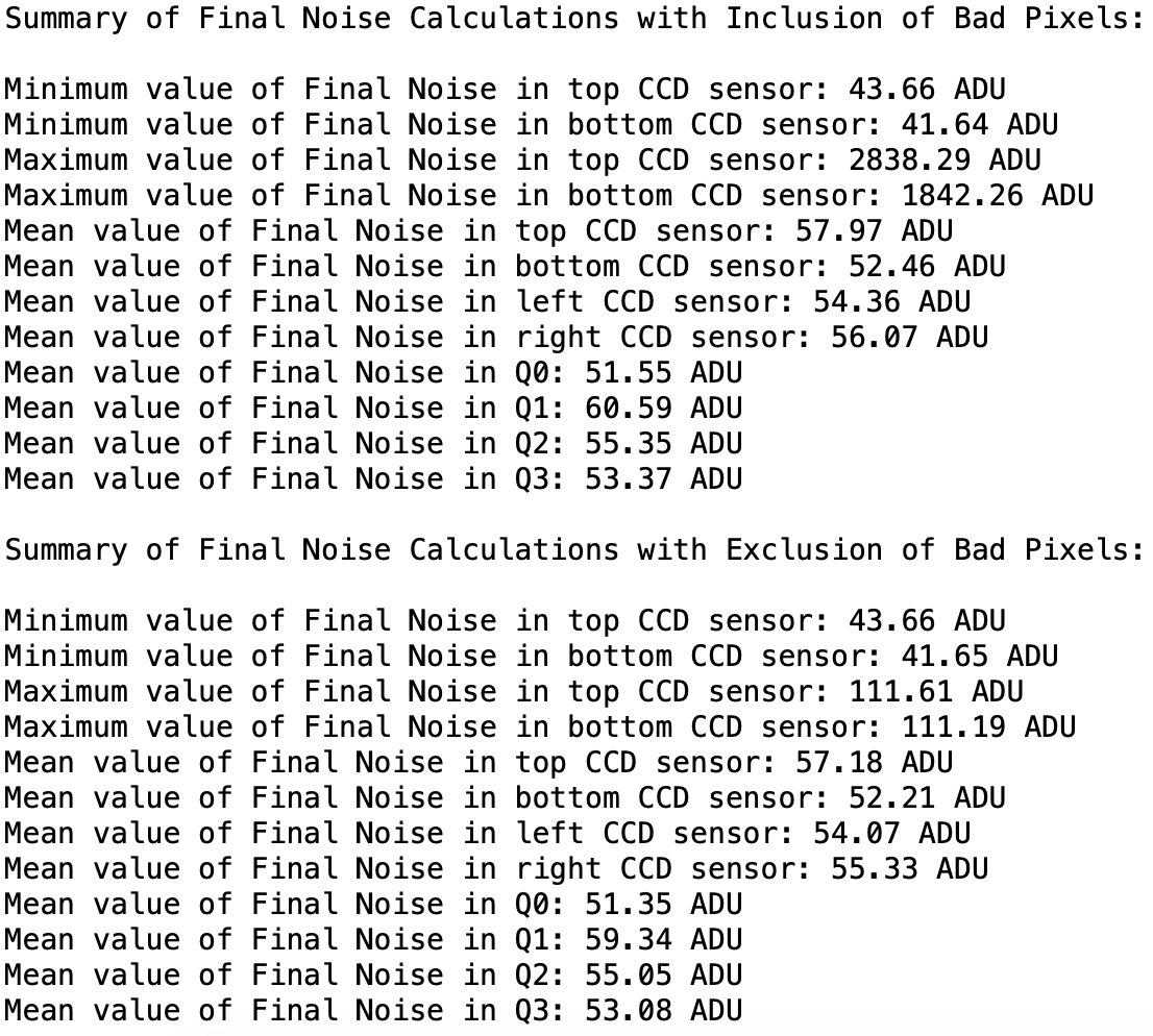
Elimination of the bad pixels from data before calculation of the final noise must be done. Fig. 3.35 and Fig. 3.36 show the heat map and histogram of the final noise map, from which our final noisy pixels could be determined. Fig. 3.37 shows an example of statistics on the final noise map with and without the bad pixels.
Fig. 3.32 The logarithm of base 2 of the bad pixels map for gain 1/1 and HDR mode of operation. Data are from run 99 of proposal 2720. |
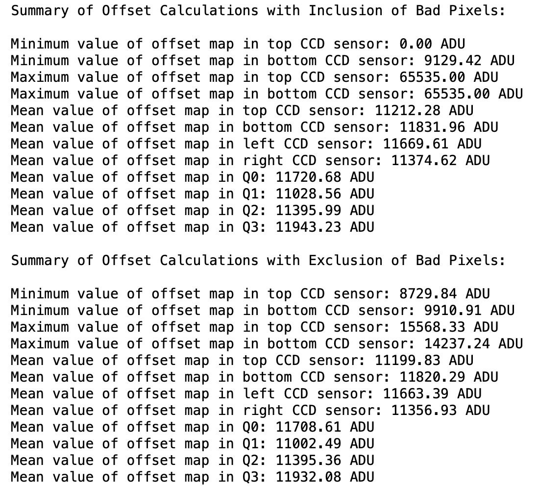
Fig. 3.33 The effect of masking bad pixels on the statistics (over all pixels) of dark offset map. Data are from run 99 of proposal 2720, which is a dark run with gain 1/1. pnCCD was in the HDR mode of operation.
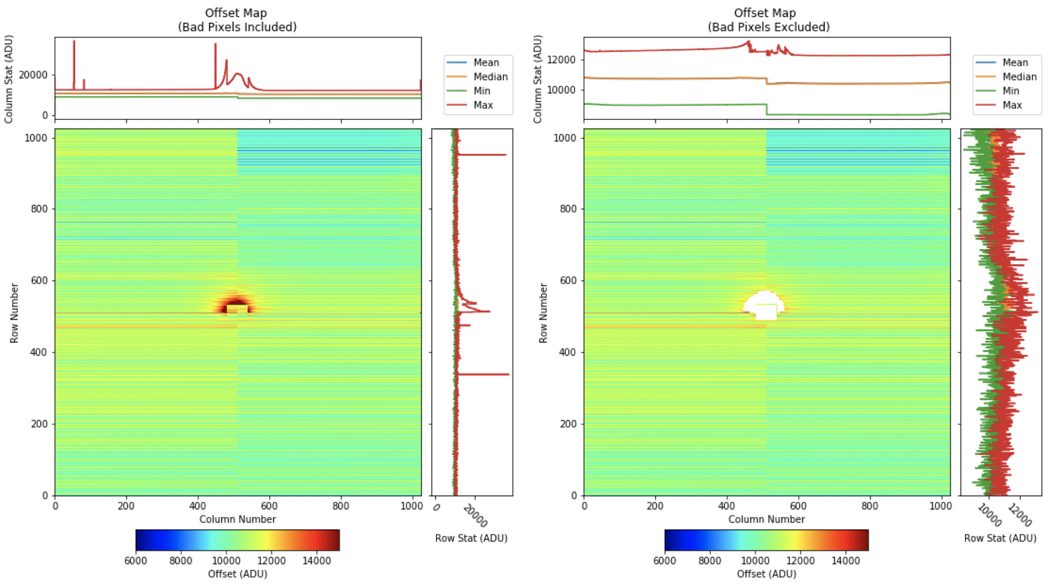
Fig. 3.34 (Right) Offset map with bad pixels included, and (left) same offset map with bad pixels excluded for HDR mode of operation with bias voltage of \(- 470\) V and gain configuration of 1/4. Data are from run 127 in proposal 2714.
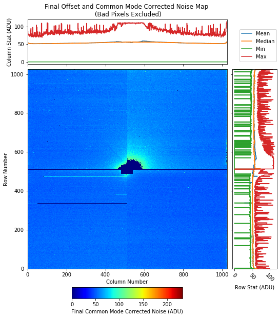
Fig. 3.35 When we exclude all bad pixels from the dark data prior to correcting the dark offset and performing a common mode correction on the offset corrected data, we obtain the final noise map. This noise map is the best estimation of the actual noise. Data are from run 99 in proposal 2720. Gain was set to 1/1 and, the pnCCD was in HDR mode of operation.
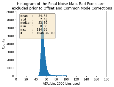
Fig. 3.36 Histogram of the final noise map after exclusion of the bad pixels and applying offset and common mode corrections to the dark data. The standard deviation of this distribution is further reduced (in comparison with Fig. 3.29) due to the exclusion of the bad pixels. Data are from run 99 in proposal 2720. Gain \(=\) 1/1 (HDR mode).
3.6.2. Effect of Masking Bad Pixels on the Corrected Data
Eliminating bad pixels prior to offset and common mode corrections of the dark data has a noticeable effect on the final corrected signal. Namely, the standard deviation is further reduced (see Table 3.10).
3.7. Injecting Dark Constants to the Calibration Database
After processing each dark run (see pnCCD Operation Manual), three maps , which are so-called dark constants, are injected into the European XFEL calibration database. These maps are the offset, noise, and bad pixels maps. These dark constants could be retrieved from the calibration database when i) an illuminated run needs to be corrected and processed (see IlluminatedCorrection), and ii) for the online preview (see pnCCD Operation Manual).
Before injecting dark constants to the calibration database, each constant (offset, noise, and bad pixels maps) is tagged with the detector size (1024 by 1024 pixels), temperature in Kelvin, bias voltage, pnCCD gain, and a creation time. The latter is the time when the dark constants are successfully injected into the calibration database. This happens when the pnCCD dark analysis notebook is successfully ran to its end for a particular dark run and that run is processed such that the dark constants associated to that dark run are obtained.
If a dark run is processed twice and the dark constants were successfully injected to the calibration database on the first trial, they will not be injected again on the second trial. One has to ask the calibration team of the detector group to disable a set of dark constants associated to a particular dark run before one can inject them again with the same conditions.
During the retrieval process of dark constants, the calibration database is searched for conditions such as detector size, temperature, bias voltage, pnCCD gain, and creation time of dark constants. The calibration database then picks the constants with the desired conditions such that the creation time is closest in time to the time of retrieval of the constants, and the temperature could be any value within \(\pm\) 5 degrees Kelvin from the temperature used to tag the constants upon their injection to the calibration database.
3.8. Concluding Remarks and Recommendations
- We recommend that the dark runs, regardless of the pnCCD gain, are obtained for 500 trains, which would result in 500 frames. The number of trains can be counted using the sequencer counters. One can clear the sequencer, start the run immediately after and stop the run as soon as the counters show 510. Here, we assume that in between clearing the sequencer and starting the run, 10 trains are already counted. Taking the dark run for 500 trains or frames ensures that there are no empty frames at the end of the run. However, to be certain that the offset is not wrongly calculated due to possible empty frames, make sure that your algorithm searches for and excludes empty frames before calculating the offset.
- The stability of the dark offset as a function of time (without power cycling the detector) is not vigorously studied yet. This should be carried out in the future to examine whether or not the dark offset shifts over time if the detector’s conditions (such as bias voltage, gain and temperature) remain the same.
- Several dark runs were analyzed with different gains and bias voltages. As a result, sometimes we observe that the offset corrected dark signal is modulated with a periodic signal with an amplitude of up to 800 ADU (peak-to-valley) as shown in Fig. 3.22. The amplitude of the modulation changes from frame to frame and from column to column. This modulation originates in a periodic change of the baseline due to the common mode effect of the individual CCD columns. The frequency of this modulation can change from run to run. The distribution of this common mode is mostly (but not always) a Gaussian distribution, whose full width at half maximum could be over a couple of hundred ADUs broad depending on the gain factor of the pnCCD (see Table 3.4 to Table 3.5). With decreasing the gain factor, the full width at half maximum of the common mode distribution gets narrower and amounts to typical values of \(\approx\) 2 to 5 ADU and slightly changing from run to run. The applied column-by-colume common mode correction can partially compensate for the baseline variation in column direction.

|
|
- The pnCCD notebooks developed at European XFEL are capable of providing the time and frequency distribution of common mode values per quadrant in order to identify and remove the possible external parasitic frequencies.
- We do not apply an electronics saturation threshold (signal values \(\geq\) 65635 ADU due to 16-bit ADCs) for identifying bad pixels. This is because the CCD full well capacity (see
ChapterThree) limit will be reached well before the former saturation is reached. We analyzed a few dark and illuminated runs with different gains and operation modes and it does not look like the data show many pixels with signals above electronics saturation limit for any of the raw images used to calculate the offset and noise maps.
