4. Characterization of Illuminated Data
When X-ray photons hit the pnCCD, some (or all) pixels register photon events resulting in illuminated images. To correct these images, we follow certain algorithms which are described in this chapter.
4.1. Data Corrections for Illuminated Runs
The first step for correcting the illuminated images is to search and remove any empty frames that may exist in the raw data. After that, we apply the bad pixels map to each raw image frame to mask any noisy pixel and events caused by cosmic rays, etc. The bad pixels map is obtained from a dark run taken with similar detector conditions (bias voltage, gain, temperature) as those of the illuminated run.
After applying the bad pixels map to the data, the next step is offset correction, which is done by subtracting the offset (obtained from the dark run) per pixel for all image frames (one at a time). The offset comes from the same dark run from which we used the bad pixels map. This dark run should preferably be taken close in time to the illuminated run to ensure that the offset correction is valid. Even though the detector conditions may be the same for the dark run and the illuminated run, if the offset varies by a bit over a long period of time, then the offset correction may not be accurate if the dark and illuminated runs are not taken close in time.
Warning
The pnCCD shows some afterglow behavior when it is illuminated by intense radiation. This makes it particularly important to take frequent dark runs in between illuminated runs to ensure correct offset subtraction.
All the aforementioned corrections explained above will always take place. What comes next depends on what additional corrections the users are interested in. The following corrections are optional and the users have the ability to turn them ON/OFF depending on their needs, as well as the availability of gain maps for photon energies of interest (see GainCorrection):
- Common mode correction
- Relative gain correction
- Split event correction and pattern classification
If common mode correction is desired, we perform a common mode correction per image frame right after offset correction. For the common mode correction step, we assume a minFrac of 0.25 (see commonMode), which means we need at least 128 usable pixels per column per quadrant to be able to perform common mode correction (see commonMode). Next, we examine the offset and common mode corrected signal per pixel per image frame to see if it is higher than a threshold. This threshold is set to 32000 ADU and comes from the full well capacity analysis (see FullWell). If the offset and common mode corrected signal per pixel per image frame is higher than this threshold, we mask the pixel with such a signal because most likely this event is not produced by any photons of interest. Masking such pixels also enusres that the common mode correction does not produce any undesired artifacts to the corrected data due to for example wrong choice of the minFrac parameter, in which case the large signals from photon events may skew the medians computed while correcting for common mode.
If relative gain correction is desired, the next step would be to correct the offset and common mode corrected data (provided that the common mode correction is turned ON) using the latest available relative gain map (see GainCorrection and Illuminated_Constants). The latter must be obtained for the photon energy of interest and detector conditions identical to the illuminated run. These conditions are bias voltage (i.e., the detector operation mode), pnCCD gain and temperature.
If relative gain correction is desired, it is performed by dividing the offset and common mode corrected data (provided that the common mode correction is turned ON) by the relative gain map per pixel for each image frame.
Note
Currently, we do not perform any charge transfer inefficiency correction to the pnCCD data because the charge transfer inefficiency is negligible for the pnCCD detector.
Finally, the last optional correction is split event correction and pattern classification, which is explained in detail in the next section. Before moving on to the next section, it is worth while to note that after each correction, we save the corrected data into a database with a separate path, and all these databases are saved in one corrected file. These files are found under the proc/ directory under each proposal directory.
To access the corrected data, one can open the separate databases mentioned above using the following paths:
- Raw data prior to any corrections:
/INSTRUMENT/SQS_NQS_PNCCD1MP/CAL/PNCCD_FMT-0:output/data/image
- Bad pixels map:
/INSTRUMENT/SQS_NQS_PNCCD1MP/CAL/PNCCD_FMT-0:output/data/mask
- Offset corrected data:
/INSTRUMENT/SQS_NQS_PNCCD1MP/CAL/PNCCD_FMT-0:output/data/pixels
- Common mode corrected data:
/INSTRUMENT/SQS_NQS_PNCCD1MP/CAL/PNCCD_FMT-0:output/data/pixels_cm
- Relative gain corrected data:
/INSTRUMENT/SQS_NQS_PNCCD1MP/CAL/PNCCD_FMT-0:output/data/gain
- Split event corrected data:
/INSTRUMENT/SQS_NQS_PNCCD1MP/CAL/PNCCD_FMT-0:output/data/pixels_classified
- The patterns resulting from the pattern classification algorithm:
/INSTRUMENT/SQS_NQS_PNCCD1MP/CAL/PNCCD_FMT-0:output/data/patterns
These paths are saved in files whose names are like CORR-R0354-PNCCD01-S00005.h5, where 354 is the run number and 5 is the sequence number (every 500 trains will construct one sequence of raw data saved to disk). These files are produced for any run which has been processed through Meta Data Catalog or by running the pnCCD correction notebook.
4.1.1. Split Event Correction and Pattern Classification
Photons impinging on a semiconductor detector will create an average number of electrons determined by:
where \(E\) is the energy deposited in the active sensor volume and \(\epsilon\) is a material specific constant determining the number of electron-hole pairs created per deposited energy unit. For silicon this constant is \(3.6\;\mathrm{eV/e^{-}}\).
In a CCD, the created charge drifts towards the readout structure according to the applied bias potential. During this drift time, latteral diffusion of the charge occurs, leading to charge being distributed over a non-negligable volume at the time of collection. This charge volume is frequently referred to as the charge cloud. Due to the cloud’s lateral extension of usually a few tens of micrometers, charge may be distributed over multiple pixels when the pixel size is small (as is the case for pnCCD). Each pixel will thus only register a fraction of the charge, corresponding to a fraction of the deposited energy.
Another effect responsible for broadening of the charge cloud is electrostatic repulsion which is described by Coulomb’s law. Diffusion and electrostatic repulsion have different relative importance on the final charge cloud diameter. We assume diffusion to be the dominating effect. Fig. 4.1 shows the example of charge sharing in one pixel. There are different areas defined for which charge sharing effect can be considered. The yellow circle represents the charge cloud. If the centre of the cloud is moved through the areas marked with \(D\), \(T\) and \(Q\), charge sharing with neighbouring pixels will occur. Different areas mean a different number of pixels affected by the charge cloud. \(D\) (doubles) represents events where charge is shared in two neighbouring pixels, for \(T\) (triples), three pixels are affected and for \(Q\) (quadruples), four pixels are affected. The center area labelled with \(S\) represents the area where there is no charge sharing effect and the generated charge cloud will be detected only in one pixel. Such events with no charge sharing are called single events. For singular photon events, i.e., events which do not result in overlapping charge clouds, the total distributed energy can be reconstructed by summing the charge in the event pattern’s pixel constituents. Charge sharing is evaluated using pattern classification algorithm.
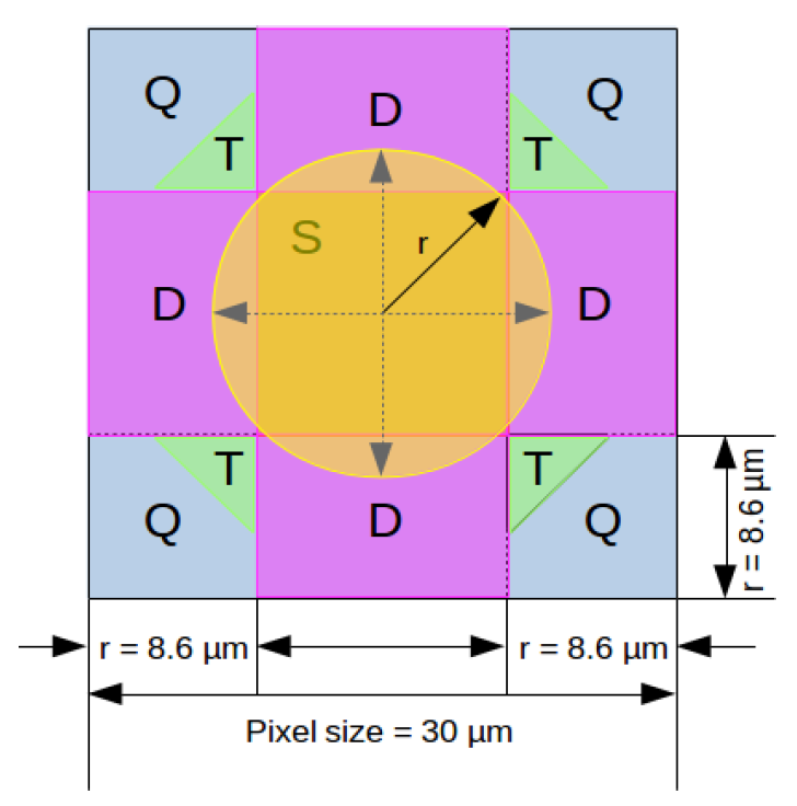
Fig. 4.1 Areas within one pixel specifed for charge sharing events. The charge cloud is represented by a yellow circle and its radius is labelled as \(r\). Note that this picture is made for the FastCCD detector, whose pixel size is much smaller than that of pnCCD. Therefore, the radius \(r\) does not indicate the size of charge cloud for pnCCD. If a photon hits the area labelled with \(S\), the resulting event pattern will be a single event. The same applies for the other areas, where \(D\) stands for doubles, \(T\) for triples and \(Q\) for quadruple event patterns. The image and caption are taken from Ivana Klačková master’s thesis p. 31).
The pattern classifier algorithm, developed by Steffen Hauf, uses an iterative algorithm to correct events which have resulted in charge sharing between multiple pixels. This is done in a multi-step process:
- The algorithm finds a pixel which has a value above a so-called primary threshold. This threshold is expected to be given in terms of \(n\times\sigma_{\mathrm{noise}}\), hence a noise map (from a dark run) also has to be supplied. The primary threshold is chosen to be \(4\sigma\).
- Within a 3 \(\times\) 3 or 4 \(\times\) 4 pixel region centered on the pixel explained above, the algorithm finds any pixels with values above a secondary threshold, given in terms of \(n\times\sigma_{\mathrm{noise}}\) as well. A 3 \(\times\) 3 region is used for single pixel events, a 4 \(\times\) 4 region is used for multi-pixel events. The secondary threshold is chosen to be \(3\sigma\). The number of pixels affected by charge splitting is referred to as an event pattern.
- The algorithm evaluates pixels above and below threshold pixels with respect to a list of i) valid patterns (see Fig. 4.2), which are pixel-charge distributions which can be created by a single impinging X-ray photon, and ii) invalid ones, which are distributions which could not have resulted from a single photon. Patterns are classified as either valid or invalid, depending on their shape. Only patterns with no direct neighbouring pattern are considered as valid. Patterns are assigned a multiplicity which corresponds to the number of pattern constituents. Valid single X-ray patterns have multiplicities 1 to 4 and the constituents form connected sub-parts of 2 \(\times\) 2 pixel square. Within each pattern, the charge distribution is additionally evaluated. For triples, the majority charge needs to be in the center pixel. For quadruples, the minority and majority charge must be diagonally opposite of each other. Valid patterns must be free-standing, i.e., no direct neighbour pixels may contain events. Diagonally offset pixels may contain events.
- If a positive match is found, the algorithm sums up the constituents and attributes the summed charge to the pixel with the majority charge. It negates all secondary constituents and values below threshold. If the summed value (in ADU) is below an upper threshold (which we assume to be 10 times the noise averaged over all pixels), pattern is considered valid. Otherwise it is attributed to a cosmic ray.
- The algorithm adds the pattern constituents to a pattern mask, indicating pattern multiplicity and orientation by an index. This pattern mask will also be used to avoid re-evalutating a pixel as part of other patterns.
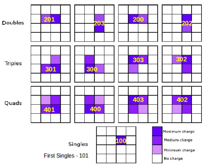
Fig. 4.2 Event patterns possibilities. Charge distribution amongst pixels is evaluated according to the displayed patterns. Each event is assigned a multiplicity with specific index as indicated in the plot. The image and caption are taken from Ivana Klačková master’s thesis (p. 46).
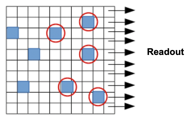
Fig. 4.3 Schematic illustration of the first single events selection. Blue squares represent single events. Events marked with a red circle are considered as the first single events in the specified direction of readout defined by the direction of arrows. The image and caption are taken from Ivana Klačková master’s thesis (p. 46).
As a result of this algorithm, information about the total energy (in ADU) of the pattern and the pattern indices of the identified patterns are produced. The patterns which have no charge sharing with neighbouring pixels are marked as single event patterns. There is an option to select from the single events only those single events which are nearest to the readout for each row. Single events nearest to the readout are so-called first single events (see Fig. 4.3). Single events are used for charge transfer inefficiency and relative gain characterizations. As there are readout ports on both sides of the pnCCD sensors, right and left hemispheres of the pnCCD are analyzed separately.
Fig. 4.2 shows the distribution of the different valid event types: singles, doubles, triples and quadruples. Event occurance depends on pixel and charge cloud size and is thus detector and application specific.
On a well corrected and configured detector, events should be isotropically distributed, except for source profile effects, which should still affect all events of a given flavor similarly. Specifically, there should not be a preferred orientation for a given event flavor visible from the pattern plots.
For the split event correction and pattern classification, we use the bad pixels map to mask the bad pixels in the data. We also consider two hemispheres for the pnCCD: left and right. We then do pattern classification separately for the left and right sides of the detector.
4.2. pnCCD Gain Calibration
The gain calibration is performed using flat-field illumination of the pnCCD via aluminium fluorescence at 1.6 keV photon energy. It is of crucial importance that the flat-field condition is maintained; otherwise, the calibration is not worthy. Flat-field condition is reached when the entire surface of the detector can be illuminated homogeniously by the incident photons. Table 4.1 compares an ideal flat-field condition achieved in August - 2020 calibration of the new pnCCD with a non-flat-field condition achieved during May - 2019 calibration of the old pnCCD.
Flat-field illumination of the pnCCD is something that the SQS beamline scientists have to achieve by spending time on tweaking the beamline parameters to accomplish a homogenious illumination of the detector.
The only calibration data we currently have are achieved by aluminium fluorescence at 1.6 keV photon energy for gains and operation modes shown in Table 4.2.
Warning
Two very important rules that need to be strictly followed during data taking for calibration runs are:
- Beam must provide flat-field illumination of the pnCCD.
- Transmission must stay below \(10\%\) if the pnCCD is operated in normal mode because at higher transmission rates, the number of single events are drastically reduced, which ruins the statistics required for calibration of the pnCCD. This is particularly true for lower gains.
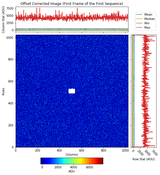
Fig. 4.4 An image showing an ideal flat-field illumination of the new pnCCD during August - 2020 calibration. Data are from run 350 in proposal 900166. Gain was set to 1/4. Detector was running in normal mode of operation. This image is offset corrected and is the first image frame of the first seuence of the run. The pnCCD is homogeniously illuminated by the incident photons. |
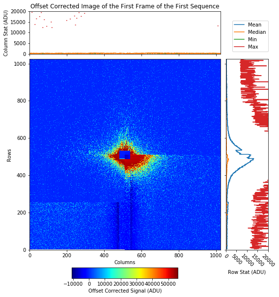
Fig. 4.5 An image showing a non-flat-field illumination of the old pnCCD during May - 2019 calibration. Data are from run 365 in proposal 900075. Gain is set to 1/1. Detector was running with bias voltage of \(-300\) V. As shown, the illumination is not homogenious. The incident photons are mostly only distributed around the center of the detector and the other parts of the detector was rarely seeing any photons. |
| pnCCD Gain | Photon Energy (keV) | Temperature Top Sensor / Bottom Sensor (degC) | Run | Dark Run | Proposal | Operation Mode | Transmission |
| 1/1 | 1.6 | -30 / -25.9 | 347 | 345 | 900166 | Normal | 9.37 |
| 1/4 | 1.6 | -30 / -25.9 | 350 | 349 | 900166 | Normal | 9.37 |
| 1/16 | 1.6 | -30 / -25.8 | 352 | 351 | 900166 | Normal | 9.37 |
| 1/64 | 1.6 | -30 / -25.8 | 354 | 353 | 900166 | Normal | 9.37 |
| 1/64 | 1.6 | -30 / -25.8 | 355 | 353 | 900166 | Normal | 50 |
| 1/256 | 1.6 | -30 / -25.7 | 360 | 356 | 900166 | Normal | 100 |
| 1/64 | 1.6 | -30 / -32 | 364 | 363 | 900166 | HDR | 20 |
| 1/256 | 1.6 | -30 / -31.6 | 366 | 365 | 900166 | HDR | 10 |
| 1/340 | 1.6 | -30 / -31 | 368 | 367 | 900166 | HDR | 50 |
4.2.1. Finding Singles Events
Once the calibration runs are corrected for offset and common mode, they are then corrected for charge split events and a pattern classification is performed for these corrected data (see Table 4.3, Fig. 4.8, and Fig. 4.9), which then identifies all valid events (see Fig. 4.10). Once the valid events for a particular run are identified, one can obtain their spectra by histogramming each of these pattern flavors. Fig. 4.11 shows an example of such spectra for only 500 image frames.
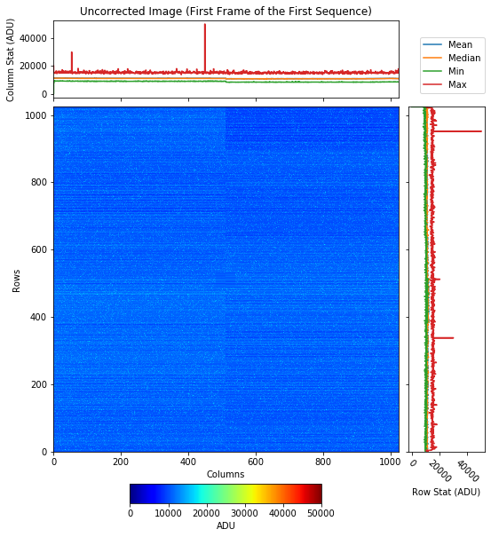
Fig. 4.6 An example showing a raw uncorrected image. Data are from run 350 in proposal 900166. Gain was set to 1/4. Detector was running in normal mode of operation. This is the first frame out of 500 frames of sequence 0 of run 350. |
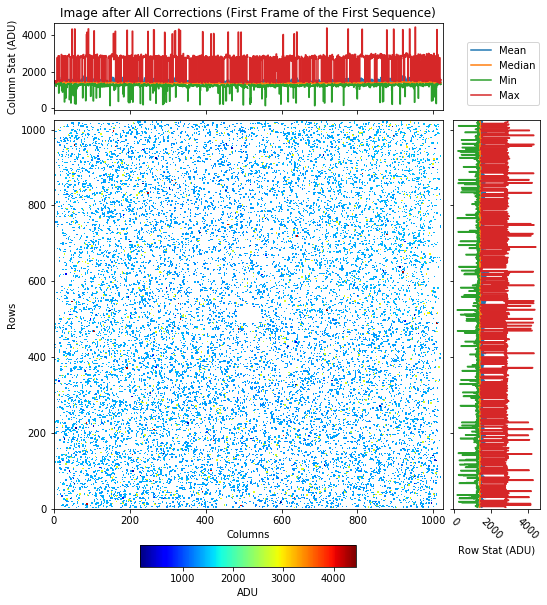
Fig. 4.7 An example showing the image of single events after offset, common mode and split event corrections are performed. Data are from run 350 in proposal 900166. Gain was set to 1/4. Detector was running in normal mode of operation. This is the first frame out of 500 frames of sequence 0 of run 350. Distribution of single events are isotropic, which indicates an ideal flat-field measurement. |
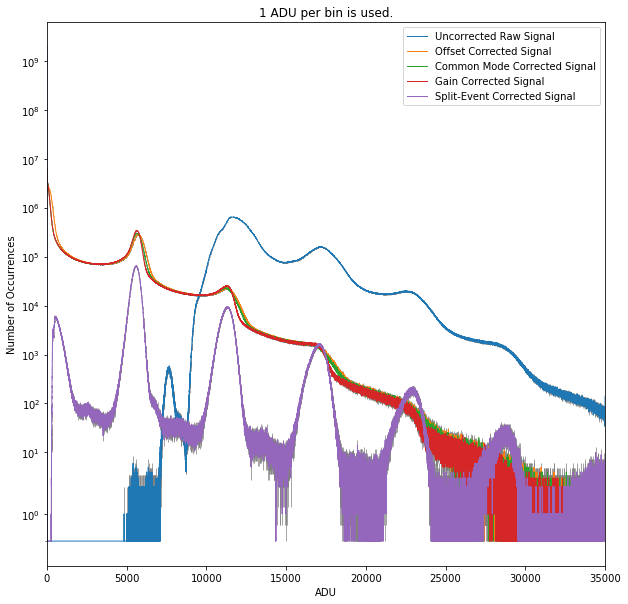
Fig. 4.8 Example of histograms of corrected and uncorrected raw data. Data are from run 347 of proposal 900166. The gain was set to 1/1 and the detector was running in normal mode of operation. This is one of the calibration runs taken in August - 2020. The noise peak centered around zero is cut due to the thresholds applied for pattern recombination analysis. The first peak, which appears around 5000 ADU, is the \(k_{\alpha1}\) line of alumimum at 1.486 keV. Other peaks are two-photons peak, etc.
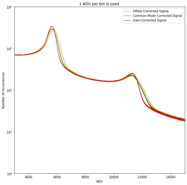
Fig. 4.9 Example of histograms of corrected data zoomed in. Gain correction improves the position of the peaks and make the peaks narrower. Data are from run 347 of proposal 900166. The gain was set to 1/1 and the detector was running in normal mode of operation. This is one of the calibration runs taken in August - 2020.
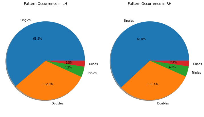
Fig. 4.10 Example of statistics of valid events. LH and RH stand for left hemisphere and right hemisphere, respectively. Data are from run 347 of proposal 900166. The gain was set to 1/1 and the detector was running in normal mode of operation. This is one of the calibration runs taken in August - 2020.
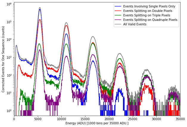
Fig. 4.11 Spectra of all valid events for run 347 of proposal 900166. The gain was set to 1/1 and the detector was running in normal mode of operation. This is one of the calibration runs taken in August - 2020. One sequence is equivalent to 500 image frames. The counts in the spectra are summed over the entire pnCCD detector. The first peak, which appears around 5000 ADU, is the \(k_{\alpha1}\) line of alumimum at 1.486 keV. Other peaks are two-photons peak, three-photons peak, etc.
We single out the single events and only work with those events for the rest of the analysis, i.e., charge transfer inefficiency and gain calibration. This is because the single events are simpler to deal with due to no charge sharing effects.
4.2.2. Per Quadrant Spectra
The spectra shown in Fig. 4.11 are obtained for the entire detector. However, pnCCD consists of two separate sensors (top and bottom sensors) each of which is divided into two parts such that each sensor has two readouts. Therefore, we are left with 4 quadrants and it would be better to acquire spectra per quadrant so we can examine the performance of each quadrant separately.
To obtain per quadrant spectra, we have two choices:
- Acquiring per row spectra for each quadrant, where rows are the readout axes. This means we will have 512 spectra per quadrant. These spectra could be the sum of all valid events or just a particular pattern flavor such as single events.
- Summing over all rows’ spectra per quadrant and obtaining one spectrum per quadrant, which is the sum of all individual spectra per row for each quadrant. Again, these spectra could be the sum of all valid events or just a particular pattern flavor such as single events.
Obtaining for each quadrant the per row spectra of single events is very useful in determination of the relative gain for each row (see GainCorrection). While, obtaining the sum (ove all rows) spectrum of single events per quadrant is used for determining absolute gain (eV/ADU) and the resolution (in eV) for each quadrant (see AbsoluteGain and Resolution).
Note
- Note that the readouts in pnCCD are parallel to the rows; therefore, all pixels in one row but different columns are connected to the same electronics, and thus have the same relative gain. The latter changes accross rows.
Fig. 4.12 shows an example of per row spectra of single events for a selected quadrant and Fig. 4.13 shows an example of the sum spectra of single events for all 4 quadrants from a gain calibration run. Depending on whether or not the relative gain correction is performed on the data, these spectra may or may not show peaks whose centroids are at the same position. If the relative gain correction is not performed, one would expect the per row spectra to have peak positions around a mean value due to small relative gain differences between each row (see Fig. 4.12). If on the other hand, the relative gain correction is performed, the spectra should show peaks whose positions are pretty much the same due to the relative gain correction (see Fig. 4.28).
Finally, one can also extract the spectrum of each pixel if this is desired (see Fig. 4.14).
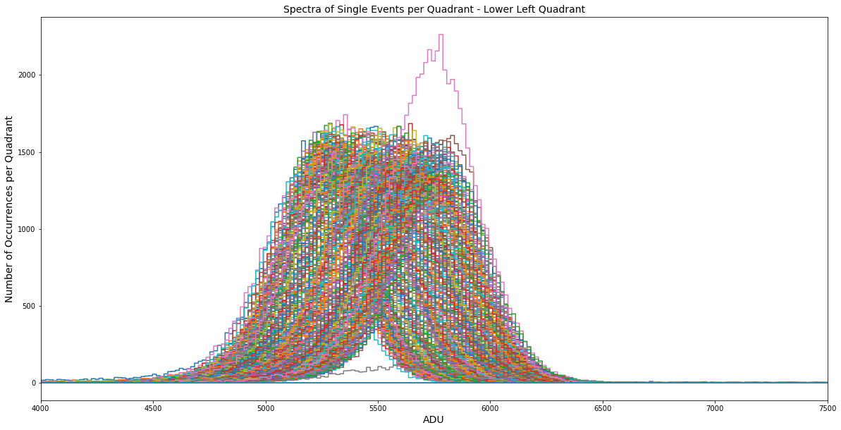
Fig. 4.12 Per row spectra of single events for lower left quadrant of pnCCD. These spectra are corrected for offset, common mode, and split event (charge sharing effect). But they are not yet corrected for relative gain. This is why, the centroid of the peak varies per row indicating small changes in relative gain from row to row. Data are taken from run 347 in proposal 900166. pnCCD gain was set to 1/1 and the detector was operated in Normal Mode. These data are from the August - 2020 calibration runs, and therefore, the peak observed in the spectra is the \(k_{\alpha1}\) line of alumimum at 1.486 keV.
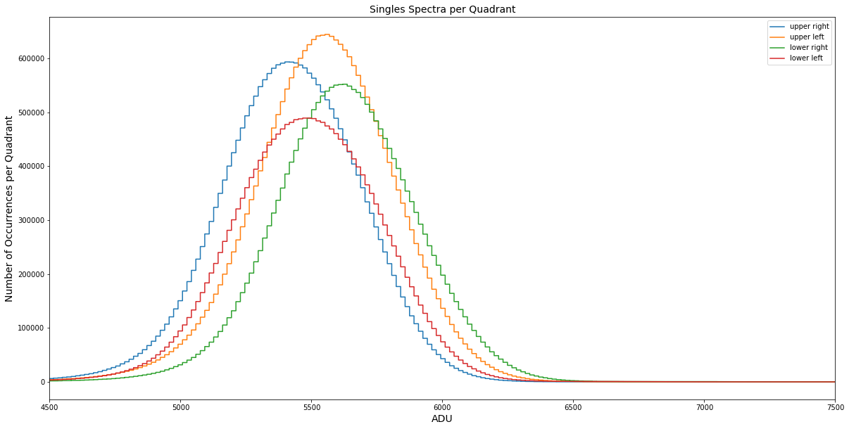
Fig. 4.13 Sum of all per row spectra of single events for each quadrant of pnCCD. The per row spectra for each quadrant are corrected for offset, common mode, and split event (charge sharing effect). But they are not yet corrected for relative gain. This is why, the centroid of the peak varies indicating small changes in an overall relative gain for each quadrant. Data are taken from run 347 in proposal 900166. pnCCD gain was set to 1/1 and the detector was operated in normal mode. These data are from the August - 2020 calibration runs, and therefore, the peak observed in the spectrum of each quadrant is the \(k_{\alpha1}\) line of alumimum at 1.486 keV.
Fig. 4.14 The figure shows the spectrum of single events from randomly selected pixels. The position of each pixel (row \(\times\) column) is given on the top right corner of each graph. Data are taken from run 347 in proposal 900166. pnCCD gain was set to 1/1 and the detector was operated in normal mode. These data are from the August - 2020 calibration runs, and therefore, the peak observed in the spectrum of each pixel is the \(k_{\alpha1}\) line of alumimum at 1.486 keV.
4.2.3. Charge Transfer Inefficiency
Charge Transfer Inefficiency (CTI) is the fractional loss of charge during charge transfer in a CCD due to occurrence of traps in the pixel structure. For the evaluation of CTI, usually first single events are used. The reason for such an approach is that the charge of first single events has not been modified by shifting through charge remnants of the previous shifts left in lattice defects during the CCD readout process. This is because these events take place very close to the readout nodes, and thus charge has not gone through many pixels to reach the readout node. However, the first single events are not that many, so their statistics is usually small. Therefore, to increase the statistics, we at European XFEL use all single events (normal single events together with the first single events). Another reason why to use only single pixel hits is that these events do not need to be corrected for charge sharing, which, of course, introduces an uncertainty to the reconstructed event. To evaluate the CTI, all single events corresponding to the \(k_{\alpha1}\) peak of aluminum are plotted against their position in the columns for each readout axis (row) separately (see Fig. 4.15). These data are then fitted (see Fig. 4.16) by a linear function:
where the \(y\) values are the signal values (in ADU) corresponding to the single photon event and \(x\) values are the column numbers. The CTI value is represented by the following expression:
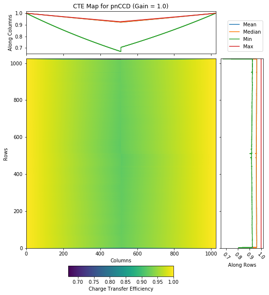
The CTI calculation algorithm allows specifying a range of values suitable for calculation. These values correspond to the minimum and maximum ADU value which define the photon peak region (in this case the \(k_{\alpha1}\) line of aluminum). The result of the CTI calculation is stored in an array containing one value of CTI for each readout axis (row), in total 512 values for one hemisphere of the pnCCD (see Fig. 4.17). This array is used for creation of a charge transfer efficiency (CTE) map (see Fig. 4.18) for the whole hemisphere as the CTE correction takes into account number of charge shifts during the readout procedure. The created CTE map can be used afterwards for correction of the CTI effects by multiplication of data and the CTE map on a per pixel basis. The CTE map contains values defined as:
where \(CTI_{(y)}\) is the value calculated by Equation (3.3) for each row of the pnCCD. The exponent \(x\) refers to the columns of the pnCCD. The value \(x\) represents the number of charge shifts needed to reach a readout node, which means \(x\) ranges from 0 to 512 for one quadrant of pnCCD. The resulting CTE map will be a 2D array with the same shape as one quadrant of the pnCCD detector. The CTE map is injected into the calibration database (see Illuminated_Constants); however, we do not currently use these maps for any data correction.
Note
- The CTI values for pnCCD are rather small and insignificant. This is attributed to the modern technologies for making silicon wafers. In modern detectors, the defects which cause charge traps in the silicon sensor are rather minimal and insignificant. When corrected, the CTE correction does not really have any noticeable effect on the images. We therefore ignore the CTE correction for pnCCD data.
- It could be the case that the fit of Equation (3.2) may not converge for a few columns such as the ones near the edges of the detector or those columns with a lot of bad pixels. Generally, if the single events statistics is poor in a column, the fit may not converge or may not be a good fit. Therefore, wherever the fit does not converge, we will set the corresponding relative gain to 1 and their CTI to the average value of the CTI in that quadrant. Generally, the number of non-convergant fits are somewhere between 4 to 17, which is a small percentange of all columns.
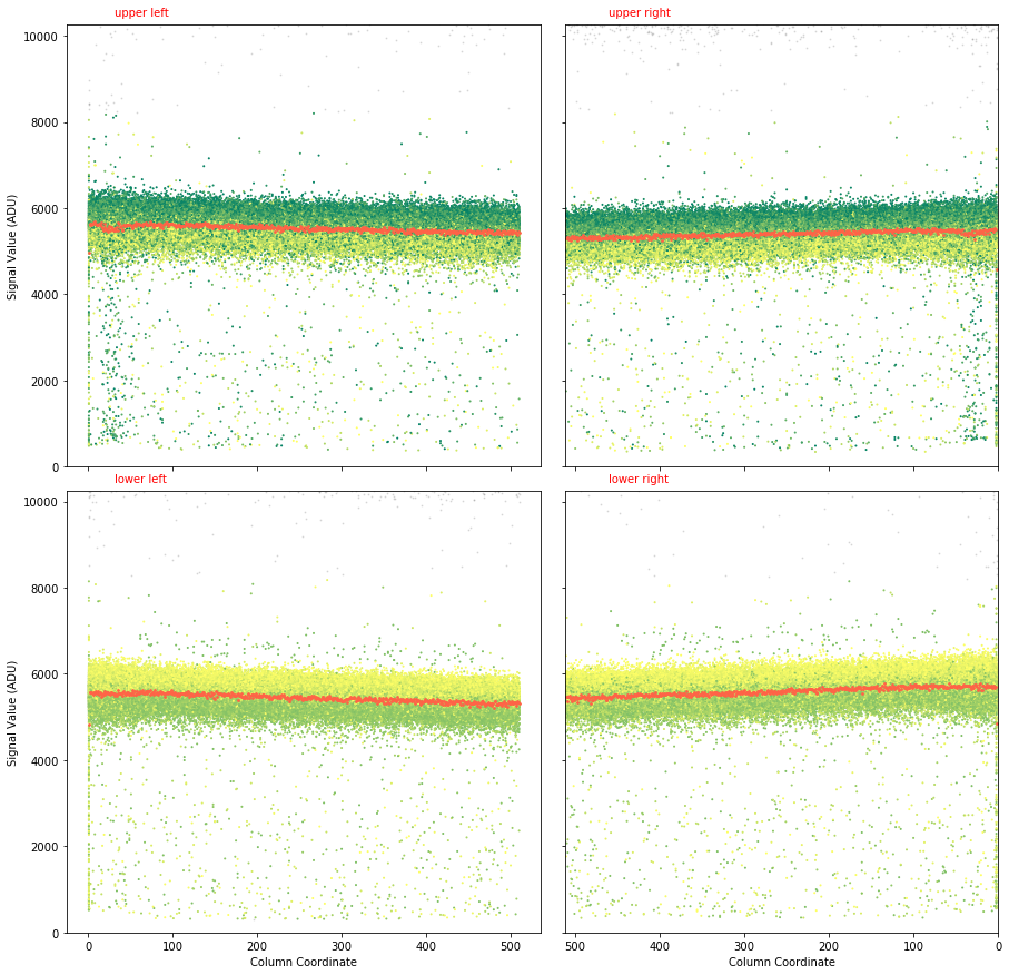
Fig. 4.15 To evaluate the CTI, all single events corresponding to the \(k_{\alpha1}\) peak of aluminum are plotted against their position in the columns for each readout axis (row) separately. The data are from run 347 in proposal 900166. The gain was set to 1/1 and the detector was running in normal mode of operation. These data are from relative gain calibration data taken in August - 2020 at 1.6 keV photon energy. The \(k_{\alpha1}\) peak of aluminum shows up around 5700 ADU (as seen on the y-axis) when pnCCD bias voltage is \(-400\) V (normal mode) and gain is set to 1/1 (highest gain). These plots show the position of 100000 selected single events from many rows in pnCCD as a function of column number per quadrant. In other words, the integrated number of photons in the emission line (e.g., the \(k_{\alpha1}\) peak of aluminum) used to determine the relative gain and CTI at 1.6 keV is 100000 photons. The color shows the intensity normalized to the maximum value (ADU) and the red line is the average signal value (in ADU).
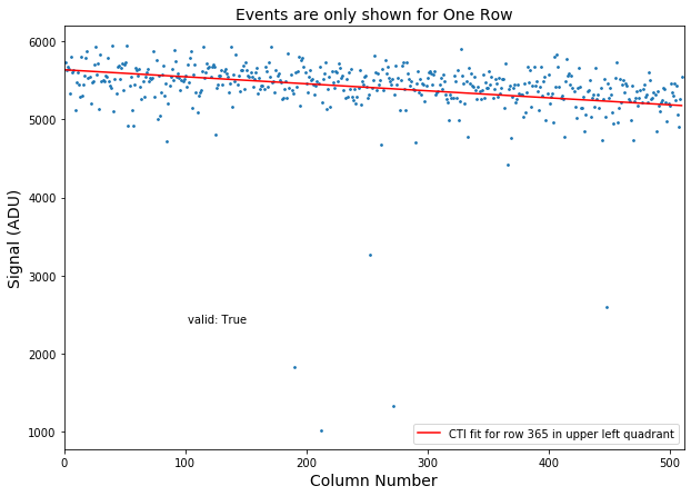
Fig. 4.16 An example of the CTI fit for a particular row (row number 365) in a particular pnCCD quadrant (upper left). Here only 512 single events corresponding to 512 columns are shown. The data are from run 347 in proposal 900166. The gain was set to 1/1 and the detector was running in normal mode of operation. These data are from relative gain calibration data taken in August - 2020. The \(k_{\alpha1}\) peak of aluminum shows up around 5700 ADU (as seen on the y-axis) when pnCCD bias voltage is \(-400\) V (normal mode) and gain is set to 1/1 (highest gain).
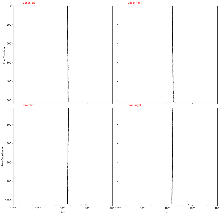
Fig. 4.17 An example of the CTI array (one value of CTI per row) per quadrant. The data are from run 347 in proposal 900166. The gain was set to 1/1 and the detector was running in normal mode of operation. These data are from relative gain calibration data taken in August - 2020. The \(k_{\alpha1}\) peak of aluminum shows up around 5700 ADU (as seen on the y-axis) when pnCCD bias voltage is \(-400\) V (normal mode) and gain is set to 1/1 (highest gain).
4.2.4. Gain Calibration Method One
In a CCD, a relative difference in the amplification of charge takes place due to the different output amplifiers for each set of readouts. For example, in pnCCD, each CAMEX contain 128 readout rows. Therefore, these 128 readout rows share the same amplification. However, the next CAMEX have different amplifiers. Eventhough, ideally these amplifiers should be identical, in practice this is not achieved.
At European XFEL, the normal method of calculating the relative gain is from the linear fit used for estimating the CTI (Equation 3.2). Relative gain is defined as:
where \(b(i)\) is the intercept of the linear fit for row \(i\), and \(N\) is the total number of columns per quadrant.
One value of relative gain will be obtained per row (see Fig. 4.19). From these values, we can obtain a relative gain map per pixel basis (see Fig. 4.20). Such relative gain maps are injected into the calibration database (see Illuminated_Constants).
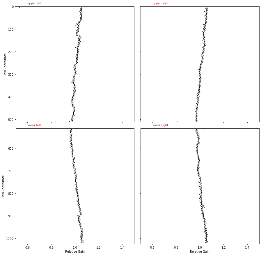
Fig. 4.19 The relative gain per row calculated for gain 1/1 of normal mode. The data are taken from run 347 in proposal 900166. This gain map is obtained using method one described in GainCorrection.
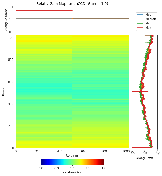
Fig. 4.20 The relative gain map for gain 1/1 of normal mode. The data are taken from run 347 in proposal 900166. This gain map is obtained based on method one described in GainCorrection.
Apart from the general method of obtaining the gain map described above, there is another way of acquiring the gain map from row-wise spectra. The latter method may be more accurate and is thus used by PNSensor as the method of obtaining their relative gain maps.
4.2.5. Gain Calibration Method Two
Once we obtain offset, common mode and split event corrected spectra for single events per row per quadrant, we can see peaks in these spectra (see Fig. 4.12). Depending on the FEL beam intensity during the calibration runs, we may be able to achive single photon zone, where only one photon hits each pixel, or we may be in multi-photons zone, where each pixel registers more than one photons. It is recommended to tune the beam such that the intensity allows single-photon zone because this would be a better calibration as identification of peaks are less troublesome. The peak observed in the spectra shown in Fig. 4.12 correspond to the \(k_{\alpha1}\) line of alumimum at 1.486 keV. If we zoom out, we will see two-photons, three-photons, etc. photo-peaks.
By fitting a Gaussian function to these photo-peaks for all rows, we can obtain another relative gain map if we subsitute the \(b(i)\) values in the numerator of Equation (3.5) by peak positions per row from the Gaussian fits, and by substituting the \(\sum_{n=0}^{N-1} b(i)\) values in the denominator of Equation (3.5) by the average peak position from all four quadrants (obtained from the Gaussian fits). The average (over all quadrants) peak position is used as a nornalization factor (hense, relative gain). A smaple of Gaussian fits is show in Fig. 4.21, and Fig. 4.22 shows the fit parameters obtained after fitting all the row-wise spectra of the lower left quadrant. These spectra are corrected for offset, common mode and split-events.
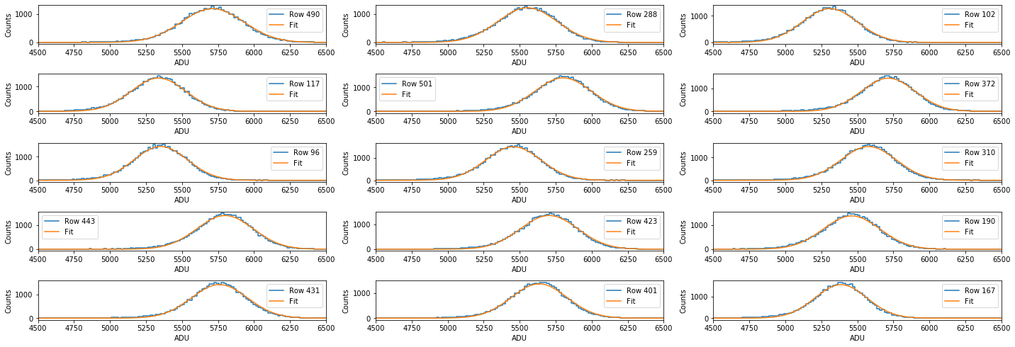
Fig. 4.21 Example of Gaussian fits for 15 randomly selected rows from the lower left quadrant on pnCCD. The peak corresponds to the \(k_{\alpha1}\) peak of aluminum. The data are taken from run 347 in proposal 900166. Gain was set to 1/1 and the operation mode was normal mode.
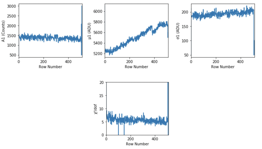
Fig. 4.22 Fit parameters obtained after fitting all the row-wise spectra of the lower left quadrant. These spectra are corrected for offset, common mode and split-events. \(A\), \(\mu\), \(\sigma\) refer to amplitude, centroid and width of each Gaussian fit, respectively. The goodness of fit is also shown on the \(\chi^{2}/dof\) plot. Data are from run 347 in proposal 900166 with gain 1/1.
Such a relative gain map is shown in Fig. 4.23. To compare this relative gain map with the one obtained from previously discussed method (see GainCorrection), see Fig. 4.24, Fig. 4.25, and Fig. 4.26. From the last two figures, one can see that the relative gain maps obtained from methods one and two are very much similar as the difference (one minus the other) between them is almost zero and the ratio of one over the other is almost one for almost all pixels.
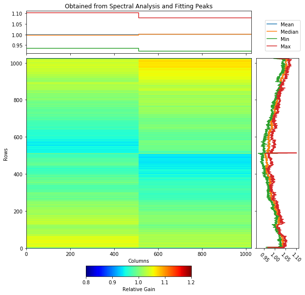
Fig. 4.23 The relative gain map for gain 1/1 of normal mode. The data are taken from run 347 in proposal 900166. This gain map is obtained based on row-wise spectra per quadrant (method two) described in GainCorrectionTwo.
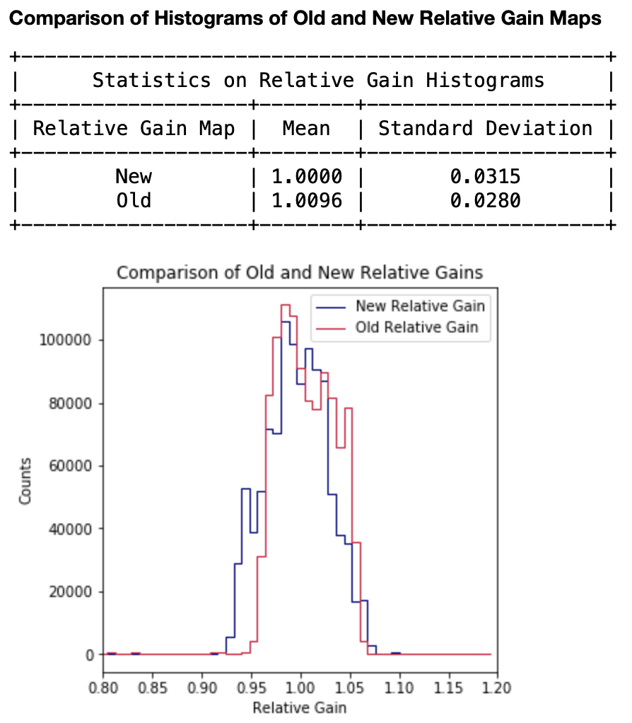
Fig. 4.24 The histograms of relative gain maps obtained from methods one (referred to as Old) and two (referred to as New). The data are taken from run 347 in proposal 900166. Gain was set to 1/1 and the detector was operating in normal mode of operation.
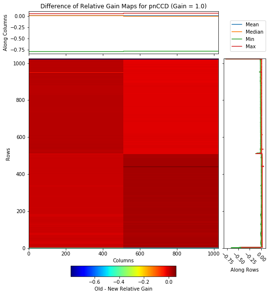
Fig. 4.25 The difference (method one minus method 2 per pixel basis) between relative gain maps obtained from methods one and two. The data are taken from run 347 in proposal 900166. Gain was set to 1/1 and the detector was operating in normal mode of operation. The difference is zero most of the times, which indicates the two relative gain maps are very similar.
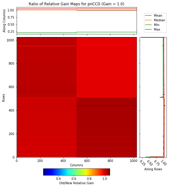
Fig. 4.26 The ratio (method one divided by method 2 per pixel basis) between relative gain maps obtained from methods one and two. The data are taken from run 347 in proposal 900166. Gain was set to 1/1 and the detector was operating in normal mode of operation. The ratio is one most of the times, which indicates the two relative gain maps are very similar.
4.2.6. Validating Relative Gain Calibration
To validate the relative gain calibration, we have two options:
- One is to use the relative gain map (which can be obtained using method one, shown in
GainCorrection, or method two, shown inGainCorrectionTwo) and correct the data for relative gain. Then, obtain per row spectra of single events from the gain corrected data. These must show photo-peaks whose centroids are more or less the same because the difference in gain between readout rows is the cause of different peak positions for different readout rows. Such differences vanish when we correct for relative gain. If the photo-peak in these per row spectra are fitted using Gaussian functions, we should get a straight line if we plot position of the peak vs. row number.- Another method would be to use the relative gain maps from methods one (
GainCorrection) and two (GainCorrectionTwo) and correct the data for relative gain separately using these relative gain maps (one at a time), and then compare the final gain corrected single events spectrum (over the entire detector) which results from these two methods. Ideally, they should be identical.
The per row spectra of single events obtained from the gain corrected data are shown in Fig. 4.27 and Fig. 4.28, where gain correction is performed using the relative gain map calculated from method one and two, respectively. As you can see, the peak corresponding to the \(k_{\alpha1}\) line of alumimum at 1.486 keV lign up nicely for almost all rows in the two selected quadrants. The second peak in the spectra corresponds to the two-photons peak, and the position of this peak also ligns up nicely for every row in these quadrants. The peaks corresponding to the \(k_{\alpha1}\) line of alumimum in these spectra are separately fitted for each row using a Gaussian function, and the results are as expected: peak positions are almost identical for all readout rows (see Fig. 4.29 and Fig. 4.30).
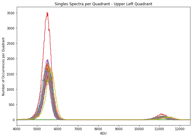
Fig. 4.27 The per row spectra of single events corresponding to the upper left quadrant of pnCCD. The spectra are obtained after relative gain correction based on method one (GainCorrection). Data are also corrected for offset, common mode and split events. Data are from run 347 in proposal 900166. Gain was set to 1/1 and the detector was in normal mode of operation. As can be seen, gain correction causes the peaks to lign up from all readout rows (shown by different colors), whereas without gain correction, the peak positions corresponding to different readout rows will not lign up (see Fig. 4.12).
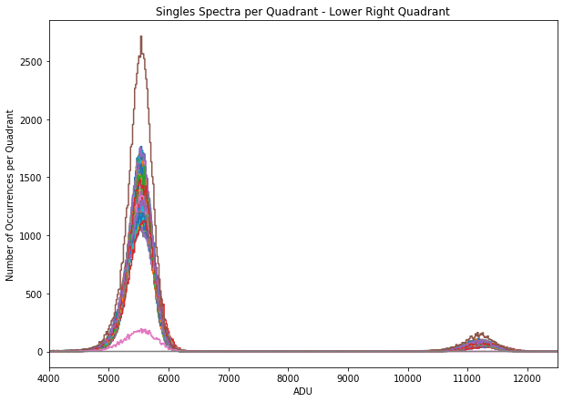
Fig. 4.28 The per row spectra of single events corresponding to the lower right quadrant of pnCCD. The spectra are obtained after relative gain correction based on method two (GainCorrectionTwo). Data are also corrected for offset, common mode and split events. Data are from run 347 in proposal 900166. Gain was set to 1/1 and the detector was in normal mode of operation. As can be seen, gain correction causes the peaks to lign up from all readout rows (shown by different colors), whereas without gain correction, the peak positions corresponding to different readout rows will not lign up (see Fig. 4.12). No matter which method we use to calculate relative gain map, the results are identical.
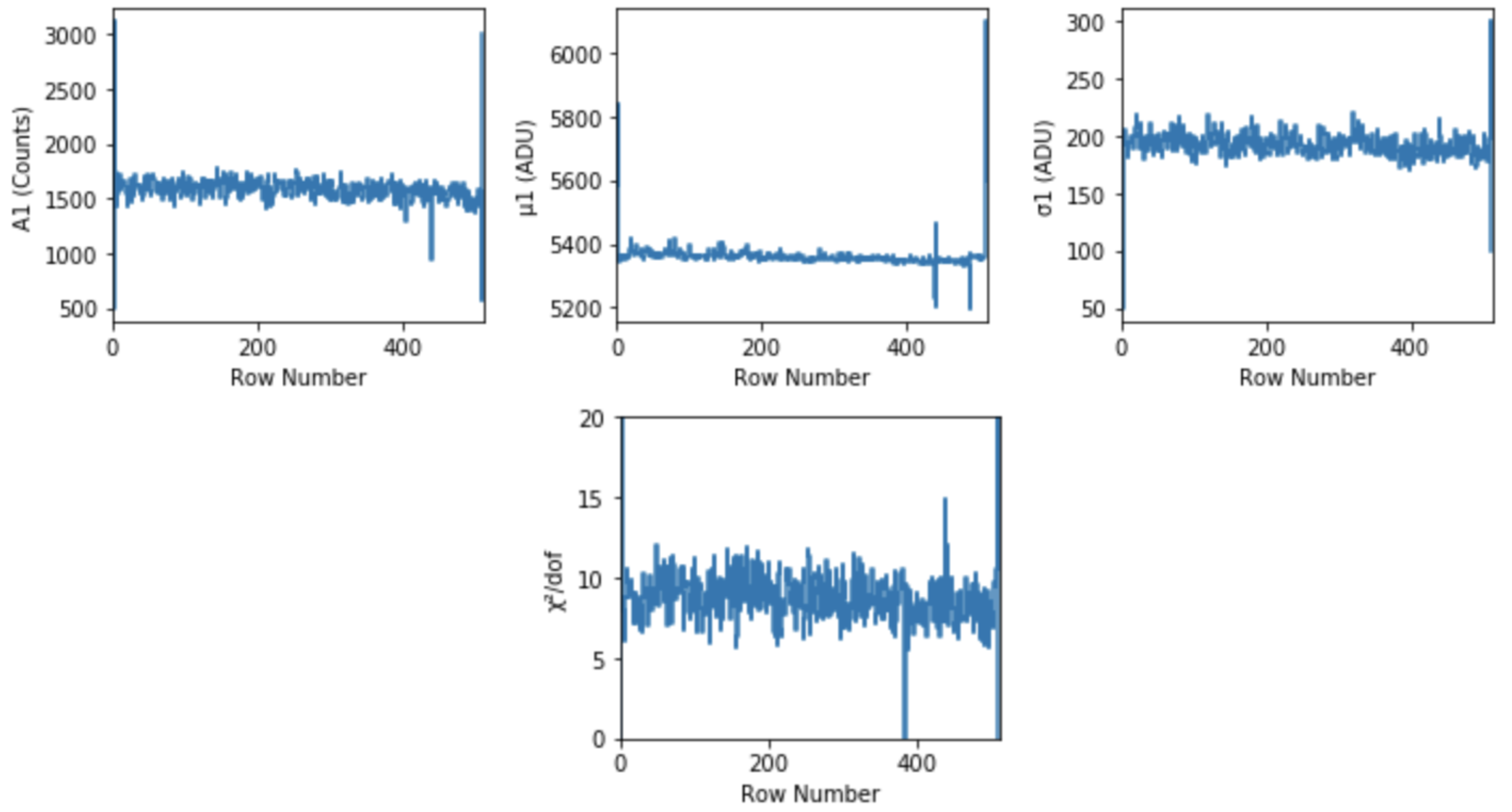
Fig. 4.29 Fitting Gassuain functions to the first peaks observed in Fig. 4.27 results in peak positions that are almost identical for all rows (as can be seen from the middle panel on the top). This is because the spectra fitted are gain corrected (based on method one). When this is not the case, the peak positions are vastly different for different readout rows as can be seen in Fig. 4.22. \(A\), \(\mu\), \(\sigma\) refer to amplitude, centroid and width of each Gaussian fit, respectively. The goodness of fit is also shown on the \(\chi^{2}/dof\) plot. Data are from run 347 in proposal 900166 with gain 1/1.
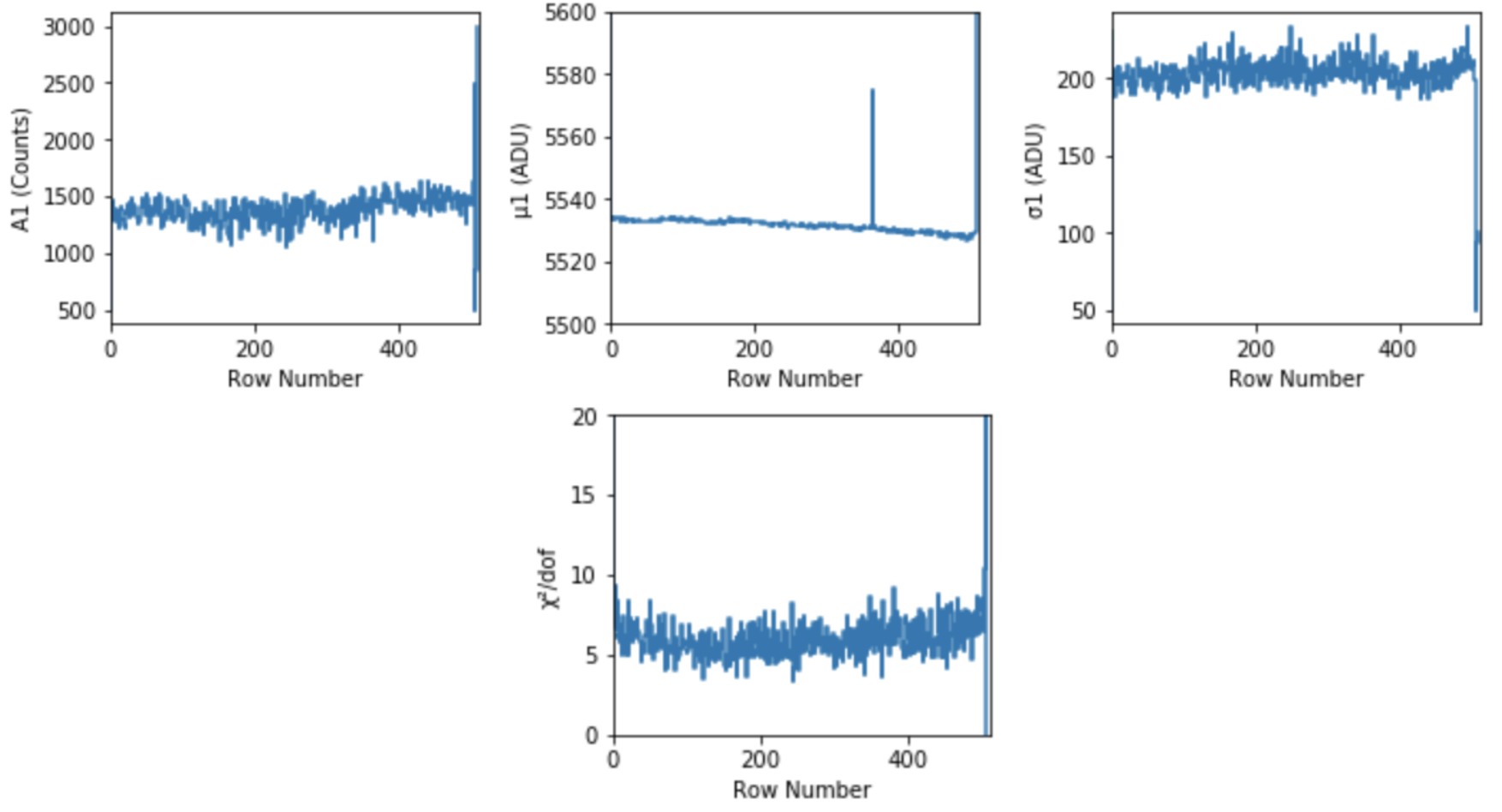
Fig. 4.30 Fitting Gassuain functions to the first peaks observed in Fig. 4.28 results in peak positions that are almost identical for all rows (as can be seen from the middle panel on the top). This is because the spectra fitted are gain corrected (based on method two). When this is not the case, the peak positions are vastly different for different readout rows as can be seen in Fig. 4.22. \(A\), \(\mu\), \(\sigma\) refer to amplitude, centroid and width of each Gaussian fit, respectively. The goodness of fit is also shown on the \(\chi^{2}/dof\) plot. Data are from run 347 in proposal 900166 with gain 1/1.
Comparing Method One with Method Two:
To compare the relative gain maps we have obtained using methods one and two, we decided to show a few factors. First, let us look at the single events spectra over the entire detector as a result of gain correction. This is shown in Fig. 4.31.
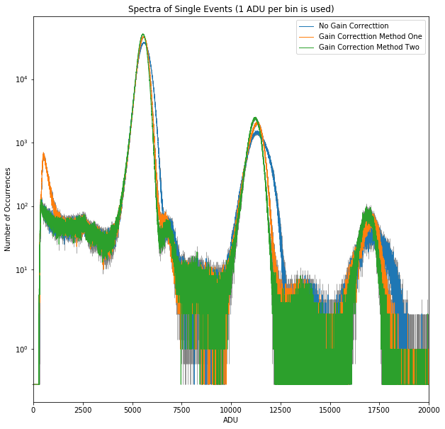
Fig. 4.31 Single events spectra obtained for data of run 347 in proposal 900166. Gain was set to 1/1 and the mode of operation was normal mode. The peaks observed are the \(k_{\alpha1}\) line of alumimum (left peak), the two-photons peak (in the middle) and the three-photons peak (on the right). Regardless of the method used for calculating the relative gain map, relative gain correction makes the peaks sharper and reduces the widths of the peaks. It also changes the position of the centroids a little bit. It seems that methods one and two are almost identical. However, method two results in the narrowest peaks (best energy resolution).
Now, let us look at what happens to the map (per pixel basis) of peak position for the peak corresponding to the \(k_{\alpha1}\) line of alumimum. Fig. 4.32 and Fig. 4.33 compare the position maps derived after gain correction using methods one and two, respectively.
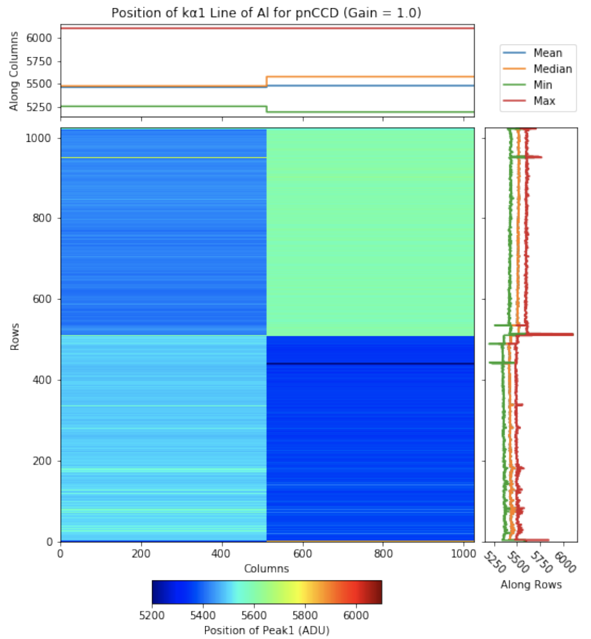
Fig. 4.32 Position (in ADU) of the peak corresponding to the \(k_{\alpha1}\) line of alumimum. The data are from run 347 in proposal 900166. Gain was set to 1/1 and the mode of operation was normal mode. Prior to obtaining this plot, the data are gain corrected using a relative gain map obtained from method one. As can be seen, the position remains more or less constant in each quadrant. However, different quadrants have different average positions.
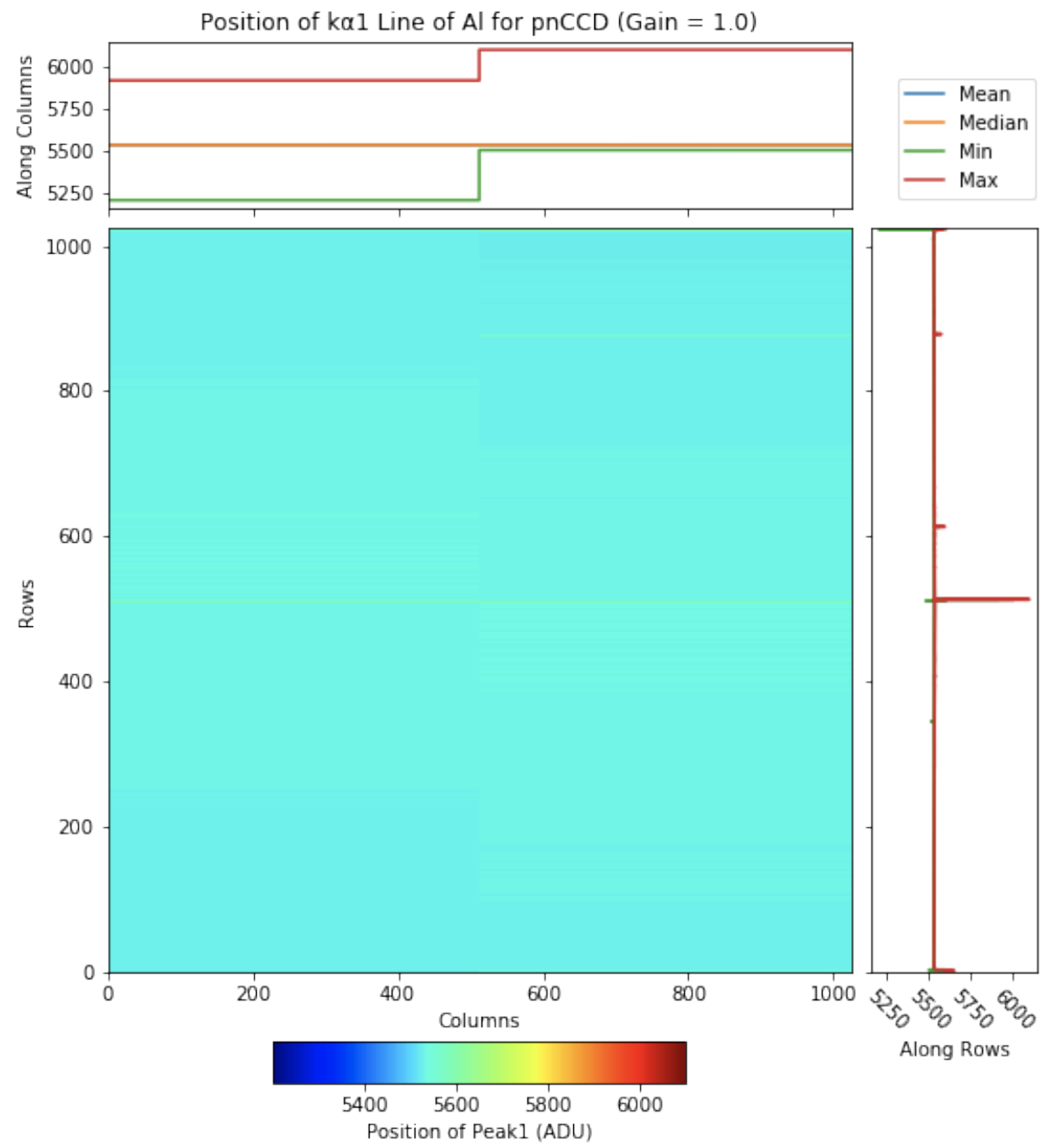
Fig. 4.33 Position (in ADU) of the peak corresponding to the \(k_{\alpha1}\) line of alumimum. The data are from run 347 in proposal 900166. Gain was set to 1/1 and the mode of operation was normal mode. Prior to obtaining this plot, the data are gain corrected using a relative gain map obtained from method two. As can be seen, the position remains more or less constant accross the entire detector.
The two methods for calculating the relative gain maps have one distinctive difference, which is described below.
If we correct the data based on the relative gain map obtained from method one, and then obtain the single events spectra summed over all readout rows per quadrant, we get 4 spectra whose positions are not identical (see Fig. 4.34). In other words, it seems method one fails to correct for the difference between gains of each quadrant. However, if we do the same but we use the gain map calculated based on method two, then the sum spectra for single events per quadrant will have identical positions as shown in Fig. 4.35. This seems to indicate that method two is a better choice, which may be the reason this method is also used by PNSensor for their analysis.
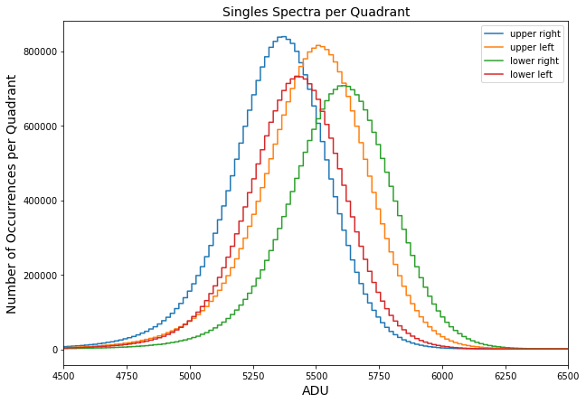
Fig. 4.34 Sum of single events spectra for all readout rows per quadrant. These spectra are gain corrected using the relative gain map obtained from method one. The data are from run 347 in proposal 900166. Gain was set to 1/1 and the mode of operation was normal mode. Since these data are gain corrected, it is confusing why the spectra are not lined up. This indicates that somehow the relative gain map from method one fails to correct for the difference between gains of each quadrant.
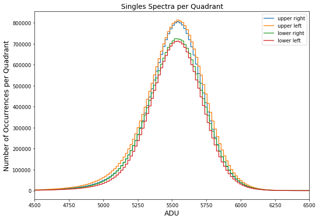
Fig. 4.35 Sum of single events spectra for all readout rows per quadrant. These spectra are gain corrected using the relative gain map obtained from method two. The data are from run 347 in proposal 900166. Gain was set to 1/1 and the mode of operation was normal mode. Since these data are gain corrected, the spectra are lined up nicely as expected. This indicates that method two may be a better method to calculate the relative gain map.
4.2.7. Absolute Gain
To calibrate the peak positions (in ADU) to energy (in eV), we need to find out the absolute gain for pnCCD detector. This is done using the spectra of single events obtained for the entire detector, as well as those obtained for the individual quadrants. The latter spectra are the sum of all row-wise single events spectra per quadrant.
From the calibration data with aluminium target at 1.6 keV photon energy, the single events spectra (over the entire detector and for individual quadrants) always show at least 3 peaks. The first one corresponds to the \(k_{\alpha1}\) line of aluminum. The second and third peaks correspond to two-photons and three-photons peaks, respectively, where two- and three-photons peaks mean that pixels have been hit by two and three photons at once (multi-photon zone).
The fits of the three aforementioned peaks from the single events spectra of lower right quadrant are shown in Fig. 4.36 to Fig. 4.38 as examples for gain 1/1 in normal mode of operation. Fig. 4.39 to Fig. 4.41 show such examples for the spectra obtained over the entire detector.
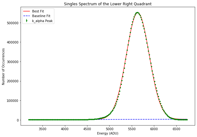
Fig. 4.36 Fitting a Guassian function to the \(k_{\alpha1}\) line of aluminum to derive its centroid and width in ADU. The data are from run 347 in proposal 900166. The gain was set to 1/1 and the pnCCD was operating in normal mode. The spectrum is summed over all row-wise spectra for lower right quadrant.
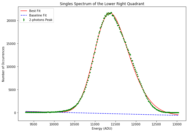
Fig. 4.37 Fitting a skewed Guassian function to the two-photons line of aluminum to derive its centroid and width in ADU. The data are from run 347 in proposal 900166. The gain was set to 1/1 and the pnCCD was operating in normal mode. The spectrum is summed over all row-wise spectra for lower right quadrant.
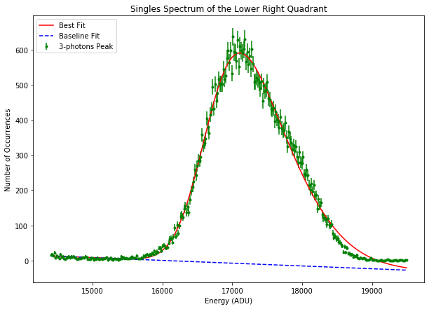
Fig. 4.38 Fitting a skewed Guassian function to the three-photons line of aluminum to derive its centroid and width in ADU. The data are from run 347 in proposal 900166. The gain was set to 1/1 and the pnCCD was operating in normal mode. The spectrum is summed over all row-wise spectra for lower right quadrant.
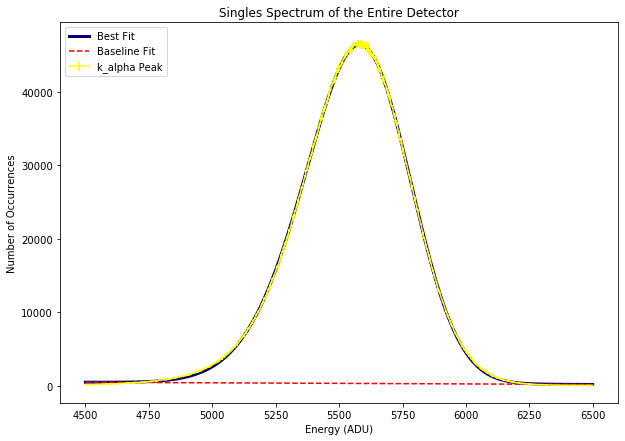
Fig. 4.39 Fitting a skewed Guassian function to the \(k_{\alpha1}\) line of aluminum to derive its centroid and width in ADU. The data are from run 347 in proposal 900166. The gain was set to 1/1 and the pnCCD was operating in normal mode. The spectrum is the single events spectrum over the entire detector.
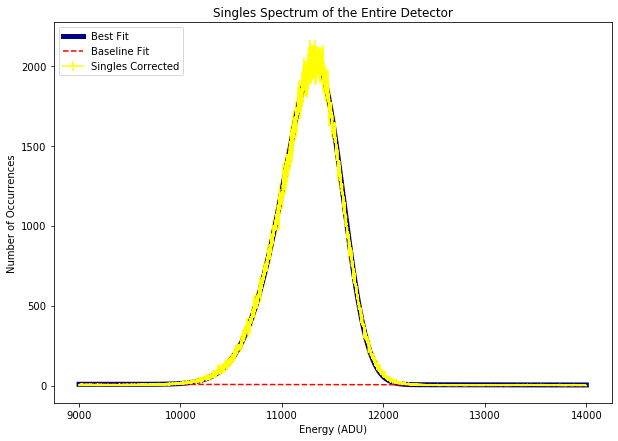
Fig. 4.40 Fitting a skewed Guassian function to the two-photons line of aluminum to derive its centroid and width in ADU. The data are from run 347 in proposal 900166. The gain was set to 1/1 and the pnCCD was operating in normal mode. The spectrum is the single events spectrum over the entire detector.
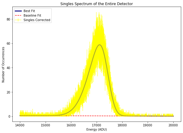
Fig. 4.41 Fitting a skewed Guassian function to the three-photons line of aluminum to derive its centroid and width in ADU. The data are from run 347 in proposal 900166. The gain was set to 1/1 and the pnCCD was operating in normal mode. The spectrum is the single events spectrum over the entire detector.
To obtain the absolute gain, we have to fit the aforementioned peaks using Gaussian or skewed Gaussian functions, depending on their shape, to acquire their centroids (in ADU) and their widths (in ADU). Knowing the energy of the associated peaks (because we have identified them as the \(k_{\alpha1}\), \(2\gamma\) and \(3\gamma\) lines of aluminum), we can convert the centroids’ ADU values to eV by plotting energies in (eV) vs. centroids (in ADU) and fitting a line with zero intercept through the data. The slope of this line is equal to the absolute gain (in eV/ADU). Table 4.4 shows the peak positions at each pnCCD gain and mode of operation.
Since the pnCCD is constructed from silicon and we know that the amount of energy required to make an electron-hole pair in silicon is 3.6 eV, we can divide the absolute gain (in eV/ADU) to 3.6 eV and obtain the conversion factor (in \(e^{-}\)/ADU). The conversion factor gives us the number of electrons released per ADU.
Examples of the linear fit, from which we obtain the absolute gain, and thus the conversion factor, are shown in Fig. 4.42 and Fig. 4.43 for gain 1/1 in normal mode of operation for lower right quadranrt and the entire detector, respectively.
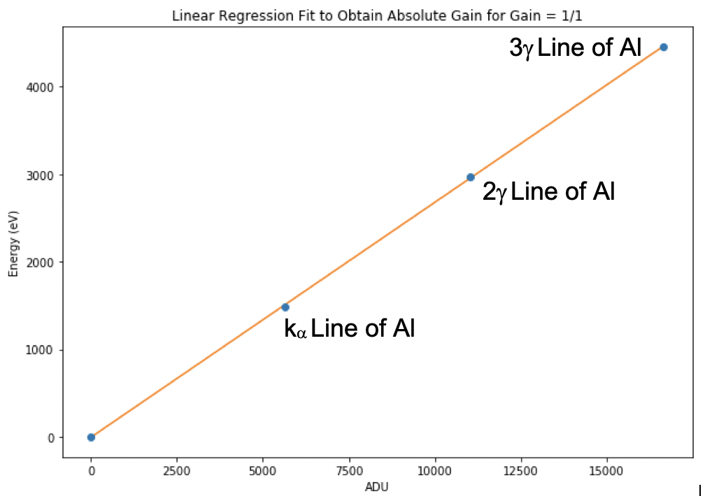
Fig. 4.42 Linear fit of energy (in eV) vs. position (in ADU) for the lower right quadrant. The data are from run 347 in proposal 900166. Gain was set to 1/1 and the detector was operating in normal mode.
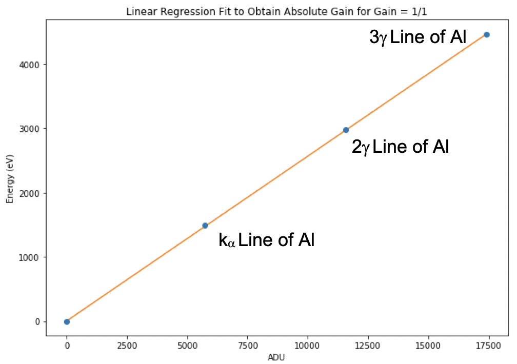
Fig. 4.43 Linear fit of energy (in eV) vs. position (in ADU) for the the entire detector. The data are from run 347 in proposal 900166. Gain was set to 1/1 and the detector was operating in normal mode.
The absolute gains and conversion factors corresponding to each available calibration are provided in Table 4.5, which is in AbsoluteGains.
| pnCCD Gain | Operation Mode | Peak 1 Position (ADU) | Peak 2 Position (ADU) | Peak 3 Position (ADU) |
| 1/1 | Normal | 5730.4 \(\pm\) 0.3 | 11564.4 \(\pm\) 0.4 | 17419.3 \(\pm\) 2.1 |
| 1/4 | Normal | 1434.4 \(\pm\) 1.2 | 2787.7 \(\pm\) 1.2 | 4201.8 \(\pm\) 1.9 |
| 1/16 | Normal | 382.4 \(\pm\) 0.1 | 756.10 \(\pm\) 0.04 | 1149.4 \(\pm\) 0.2 |
| 1/64 | Normal | 99.4 \(\pm\) 0.1 | 195.2 \(\pm\) 0.1 | 289.3 \(\pm\) 0.2 |
| 1/64 | HDR | 98.7 \(\pm\) 0.1 | 196.6 \(\pm\) 0.1 | 292.6 \(\pm\) 0.1 |
4.2.8. Detector Resolution
Once we have the absolute gain, we can use it to convert the widths of the peaks to energy, and thus obtain detector resolution. The detector resolution for pnCCD specifically refers to the eV value of the width (\(\sigma\)) of the peak associated to the \(k_{\alpha1}\) line of aluminum. This can be calculated by multipling the absolute gain by the width of this peak (in ADU). The detector energy resolutions corresponding to each available calibration are provided in Table 4.5, which is in AbsoluteGains.
4.2.9. Available Gain Calibrations for pnCCD
The available pnCCD calibrations are provided in Table 4.5.
| Gain | Operation Mode | Region | Conversion Factor (\(e^{-}/ADU\)) | Absolute Gain (eV/ADU) | \(\sigma\) (eV) |
| 1/1 | Normal | Q0 | 0.08 | 0.27092 \(\pm\) 0.00043 | 70.5 \(\pm\) 0.2 |
| Q1 | 0.07 | 0.26808 \(\pm\) 0.00078 | 68.7 \(\pm\) 0.3 | ||
| Q2 | 0.07 | 0.26268 \(\pm\) 0.00143 | 71.9 \(\pm\) 0.4 | ||
| Q3 | 0.08 | 0.27101 \(\pm\) 0.00062 | 68.8 \(\pm\) 0.2 | ||
| ED | 0.07 | 0.25659 \(\pm\) 0.00053 | 71.1 \(\pm\) 0.2 | ||
| 1/4 | Normal | Q0 | 0.3 | 1.07004 \(\pm\) 0.00240 | 70.3 \(\pm\) 0.2 |
| Q1 | 0.29 | 1.06095 \(\pm\) 0.00279 | 69.5 \(\pm\) 0.2 | ||
| Q2 | 0.29 | 1.03510 \(\pm\) 0.01110 | 71.3 \(\pm\) 0.8 | ||
| Q3 | 0.3 | 1.06447 \(\pm\) 0.00663 | 68.7 \(\pm\) 0.5 | ||
| ED | 0.29 | 1.06109 \(\pm\) 0.00426 | 74.2 \(\pm\) 0.5 | ||
| 1/16 | Normal | Q0 | 1.15 | 4.13173 \(\pm\) 0.02915 | 82.6 \(\pm\) 0.8 |
| Q1 | 1.13 | 4.07806 \(\pm\) 0.00817 | 84.9 \(\pm\) 0.5 | ||
| Q2 | 1.11 | 4.00712 \(\pm\) 0.01914 | 85.1 \(\pm\) 0.6 | ||
| Q3 | 1.12 | 4.04413 \(\pm\) 0.04071 | 82.3 \(\pm\) 1.0 | ||
| ED | 1.08 | 3.88260 \(\pm\) 0.00169 | 101.0 \(\pm\) 0.4 | ||
| 1/64 | Normal | Q0 | 4.33 | 15.60126 \(\pm\) 0.08437 | 278.9 \(\pm\) 2.9 |
| Q1 | 4.19 | 15.07336 \(\pm\) 0.08352 | 276.3 \(\pm\) 3.0 | ||
| Q2 | 4.29 | 15.42615 \(\pm\) 0.07348 | 275.6 \(\pm\) 2.8 | ||
| Q3 | 4.22 | 15.20374 \(\pm\) 0.08210 | 274.3 \(\pm\) 2.9 | ||
| ED | 4.26 | 15.33222 \(\pm\) 0.07731 | 257.3 \(\pm\) 2.9 | ||
| 1/64 | HDR | Q0 | 4.35 | 15.64482 \(\pm\) 0.04932 | 269.1 \(\pm\) 2.9 |
| Q1 | 4.17 | 15.02896 \(\pm\) 0.04307 | 269.0 \(\pm\) 3.0 | ||
| Q2 | 4.28 | 15.41863 \(\pm\) 0.03752 | 270.6 \(\pm\) 2.7 | ||
| Q3 | 4.22 | 15.20813 \(\pm\) 0.04340 | 265.8 \(\pm\) 2.7 | ||
| ED | 4.22 | 15.19430 \(\pm\) 0.03813 | 247.1 \(\pm\) 2.7 |
4.3. Injecting Illuminated Constants to the Calibration Database
The available CTE maps and relative gain maps are injected to the calibration database of European XFEL everytime the pnCCD detector is calibrated using specific commissioning beamtimes. Regardless of which method is used to calculate the relative gain map, it can be injected into the calibration database. These relative gain maps, as well as the CTE maps, are tagged by a creation time, detector size (1024 by 1024 pixels), photon energy, bias voltage, pnCCD gain, and temperature (in units of Kelvin). Just like the dark constants (see Injection), a relative gain map with a set of tags (conditions) can only be injected into the calibration database once. Also, during the retrieval process of a relative gain map, the calibration database is searched for conditions such as detector size, temperature, bias voltage, pnCCD gain, photon energy, and creation time of the relative gain map. The calibration database then picks the constants with the desired conditions such that the creation time is closest in time to the time of retrieval of the relative gain map, and the temperature could be any value within \(\pm\) 5 degrees Kelvin from the temperature used to tag the relative gain map upon its injection to the calibration database. The relative gain map, as well as the CTI map (see CTI) are called illuminated constants.
